Table of contents
Keywords: Battery, Vreg, LDOP, LDON, Flipped voltage follower, Buck, Boost, Load, Line, PSRR, MAX C, Quiescent, Settling, Efficiency, PWM, PFM
Voltage source
Most, if not all, integrated circuits need a supply and ground to work.
Assume a system is AC powered. Then there will be a switched regulator to turn wall AC into DC. The DC might be 48 V, 24 V, 12 V, 5 V, 3 V 1.8 V, 1.0 V, 0.8 V, or who knows. The voltage depends on the type of IC and the application.
Many ICs are battery operated, whether it’s your phone, watch, heart rate monitor, mouse, keyboard, game controller or car.
For batteries the voltage is determined by the difference in Fermi level on the two electrodes, and the Fermi level (chemical potential) is a function of the battery chemistry. As a result, we need to know the battery chemistry in order to know the voltage.
Linden’s Handbook of Batteries is a good book if you want to dive deep into primary (non-chargeable) or secondary (chargeable) batteries and their voltage curves.
Some common voltage sources are listed below.
| Chemistry | Voltage [V] | |
|---|---|---|
| Primary Cell | LiFeS2 , Zn/Alk/MnO2 , LiMnO2 | 0.8 - 3.6 |
| Secondary Cell | Li-Ion | 2.5 - 4.3 |
| USB | - | 4.0 - 6.5 (20) |
The battery determines the voltage of the “electron source”, however, can’t we just run everything directly off the battery? Why do we need DC to DC converters or voltage regulators?
Turns out, transistors can die.
Today’s transistor, as shown below, are a complicated three dimensional structure. Dimensions are measured in nano-meter, which makes the transistors fragile.
In Analog Circuit Design in Nanoscale CMOS Technologies 1 Lanny explains how to design around some of the breakdown effects.
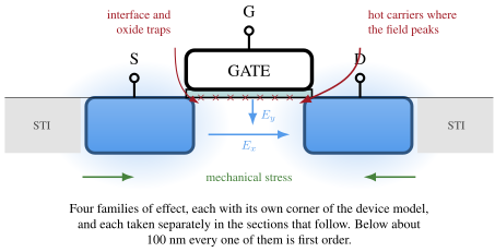
Figure 1: A nanoscale NMOS in cross-section. Mechanical stress from the isolation trenches, the transverse and lateral fields in the channel, traps at the oxide interface, and hot carriers where the field peaks near the drain
Two of those four are the ones that kill it. The transverse field $E_y$ is what the gate oxide has to withstand, and the traps are the damage accumulating in it; the hot carriers at the drain end are the other. Neither is a failure you see immediately, which is what makes them dangerous - the device works, and then some months later it does not.
The transistors in a particular technology (from GlobalFoundries, TSMC, Samsung or others) have a maximum voltage that they can survive for a certain time. Exceed that time, or voltage, and the transistors die.
Why transistors die
A gate oxide will break due to Time Dependent Dielectric Breakdown (TDDB) if the voltage across the gate oxide is too large. Silicon oxide can break down at approximately 5 MV/cm. The breakdown forms a conductive channel from the gate to the channel and is permanent. After breakdown there will be a resistor of kOhms between gate and channel.
A similar breakdown phenomena is used in Metal-Oxide RRAM 2 and the SkyWater ReRAM
Below is an example of ReRAM. In the Pristine state the conductance is low, resistance is in the hundreds of mega Ohm. In a transistor we want the oxide to stay high resistive. In ReRAM, however, we apply a high voltage across the oxide, which forms a conductive channel across the oxide. Turns out, that the conductive channel can be flipped back and forth between a high resistive state, and a low resistive state to store a 1 or a 0 in a non-volatile manner.
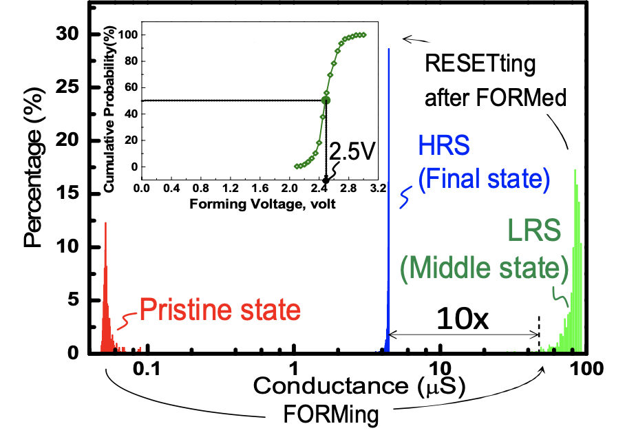
Figure 2: ReRAM conductance distributions in the pristine, formed (LRS), and reset (HRS) states. From google/skywater-pdk-libs-sky130_fd_pr_reram, Apache 2.0 license

The threshold voltage of a transistor can shift excessively over time caused by Hot-Carrier Injection (HCI) or Negative Bias Temperature Instability.
Hot-Carrier injection is caused by electrons, or holes, accelerated to high velocity in the channel, or drain depletion region , causing impact ionization (breaking a co-valent bond releasing an electron/hole pair). At a high drain/source field, and
medium gate/(source or drain) field, the channel minority carriers can be accelerated to high energy and transition to traps in the oxide, shifting the threshold voltage.
Negative Bias Temperature Instability is a shift in threshold voltage due to a physical change in the oxide. A strong electric field across the oxide for a long time can break co-valent, or ionic bonds, in the oxide. The bond break will change the forces (stress) in the amorphous silicon oxide which might not recover. As such, there might be more traps (states) than before. See Simultaneous Extraction of Recoverable and Permanent Components Contributing to Bias-Temperature Instability 3 for more details.
For a long time, I had trouble with “traps in the oxide”. I had a hard time visualizing how electrons wandered down the channel and got caught in the oxide. I was trying to imagine the electric field, and that the electron needed to find a positive charge in the oxide to cancel. Diving a bit deeper into quantum mechanics, my mental image improved a bit, so I’ll try to give you a more accurate mental model for how to think about traps.
Quantum mechanics tells us that bound electrons can only occupy fixed states. The probability of finding an electron in a state is given by the Fermi function, but if there is no energy state at a point in space, there cannot be an electron there.
For example, there might be a 50 % probability of finding an electron in the oxide, but if there is no state there, then there will not be any electron , and thus no change to the threshold voltage.
What happens when we make “traps”, through TDDB, HCI, or NBTI is that we create new states that can potentially be occupied by electrons. For example one, or more, broken silicon co-valent bonds and a dislocation of the crystal lattice.
If the Fermi-Dirac statistics tells us the probability of an electron being in those new states is 50 %, then there will likely be electrons there.
The threshold voltage is defined as the voltage at which we can invert the channel, or create the same density of electrons in the channel (for NMOS) as density of dopant atoms (density of holes) in the bulk.
If the oxide has a net negative charge (because of electrons in new states), then we have to pull harder (higher gate voltage) to establish the channel. As a result, the threshold voltage increases with electrons stuck in the oxide.
In quantum mechanics the time evolution, and the complex probability amplitude of an electron changing state, could, in theory, be computed with the Schrodinger equation. Unfortunately, for any real scenario, like the gate oxide of a transistor, using Schrodinger to compute exactly what will happen is beyond the capability of the largest supercomputers.
Core voltage
The voltage where the transistor can survive is estimated by the foundry, by approximation, and testing, and may be like the table below.
| Node [nm] | Voltage [V] |
|---|---|
| 180 | 1.8 |
| 130 | 1.5 |
| 55 | 1.2 |
| 22 | 0.8 |
IO voltage
Most ICs talk to other ICs, and they have a voltage for the general purpose input/output. The voltage reduction in I/O voltage does not need to scale as fast as the core voltage, because foundries have thicker oxide transistors that can survive the voltage.
| Voltage [V] |
|---|
| 5.0 |
| 3.0 |
| 1.8 |
| 1.2 |
Supply planning
For any IC, we must know the application. We must know where the voltage comes from, the IO voltage, the core voltage, and any other requirements (like charging batteries).
One example could be an IC that is powered from a Li-Ion battery, with a USB to provide charging capability.
Between each voltage we need an analog block, a regulator, to reduce the voltage in an effective manner. What type of regulator depends again on the application, but the architecture of the analog design would be either a linear regulator, or a switched regulator.
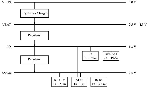
Figure 3: Example supply planning from VBUS and VBAT down to IO and core voltage, with a regulator between each domain
The dynamic range of the power consumed by an IC can be large. From nA when it’s not doing anything, to hundreds of mA when there is high computation load.
As a result, it’s not necessarily possible, or effective, to have one regulator from 1.8 V to 0.8 V. We may need multiple regulators. Some that can handle low load (nA - $\mu$A) effectively, and some that can handle high loads.
For example, if you design a regulator to deliver 500 mA to the load, and the regulator uses 5 mA, that’s only 1 % of the current, which may be OK. The same regulator might consume 5 mA even though the load is 1 uA, which would be bad. All the current flows in the regulator at low loads.
| Name | Voltage | Min [nA] | Max [mA] | PWR DR [dB] |
|---|---|---|---|---|
| VDD_VBUS | 5 | 10 | 500 | 77 |
| VDD_VBAT | 4 | 10 | 400 | 76 |
| VDD_IO | 1.8 | 10 | 50 | 67 |
| VDD_CORE | 0.8 | 10 | 350 | 75 |
Most product specifications will give you a view into what type of regulators there are on an IC. The picture below is from nRF5340 (page 23)
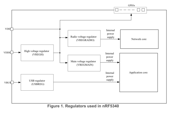
Figure 4: Regulators in the nRF5340, from the product specification. Source: Nordic Semiconductor, nRF5340 Product Specification
Linear Regulators
PMOS pass-fet
One way to make a regulator is to control the current in a PMOS with a feedback loop, as shown below. The OTA continuously adjusts the gate-source voltage of the PMOS to force the input voltages of the OTA to be equal.
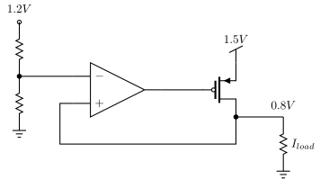
Figure 5: Linear regulator with a PMOS pass-fet controlled by an OTA feedback loop
For digital loads, where $I_{load}$ is a digital current, with high current every rising edge of the clock, it’s an option to place a large external decoupling capacitor (a reservoir of charge) in parallel with the load. Accordingly, the OTA would supply the average current.
The device between supply (1.5 V) and output voltage (0.8 V) is often called a pass-fet. A PMOS pass-fet regulator is often called a LDO, or low dropout regulator, since we only need a $V_{DSSAT}$ across the PMOS, which can be a few hundred mV.
Key parameters of regulators are
| Parameter | Description | Unit |
|---|---|---|
| Load regulation | How much does the output voltage change with load current | V/A |
| Line regulation | How much does the output voltage change with input voltage | V/V |
| Power supply rejection ratio | What is the transfer function from input voltage to output voltage? The PSRR at DC is the line regulation | dB |
| Max current | How much current can be delivered through the pass-fet? | A |
| Quiescent current | What is the current used by the regulator | A |
| Settling time | How fast does the output voltage settle at a current step | s |
A disadvantage of a PMOS is the hole mobility, which is lower than for NMOS. If the maximum current of an LDO is large, then the PMOS can be big. Maybe even 50 % of the IC area.
NMOS pass-fet
An NMOS pass-fet will be smaller than a PMOS for large loads. The disadvantage with an NMOS is the gate-source voltage needed. For some scenarios the needed gate voltage might exceed the input voltage (1.5 V). A gate voltage above input voltage is possible, but increases complexity, as a charge pump (switched capacitor regulator) is needed to make the gate voltage.
Another interesting phenomena with NMOS pass-fet is that the PSRR is usually better, but we do have a common gate amplifier, as such, high frequency voltage ripple on output voltage will be amplified to the input voltage, and may cause issues for others using the input voltage.
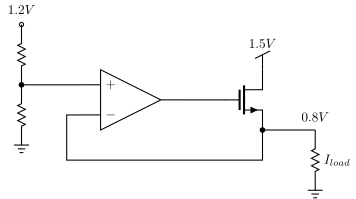
Figure 6: Linear regulator with an NMOS pass-fet controlled by an OTA feedback loop
Control of pass-fet
The large dynamic range in power management systems can make it challenging to have a single pass-fet.
The size of the pass-fet is set by the maximum Vgs, and the current that needs to be delivered.
Assume we need 500 mA from the LDO. If we assume that the maximum Vgs is 1.5 V, then we can simulate to try and find a size.
I’ve made a testbench at
Below is an excerpt from the testbench. The pass-fet size has been determined by iteration.
The OTA in the LDO is modeled by the B source. Notice the use of the tanh function in order to keep the G voltage within the rails.
* Pass-fet
XM1 OUT G VDD VDD sky130_fd_pr__pfet_01v8
+ L=0.252 W=11.52 nf=2 ...  m=1000

* Reference
VREF VREF 0 dc 0.8

* OTA
BOTA G 0 V=(1 + tanh(-1000*(v(vref) -v(out) )))/2*{AVDD}

* Load cap
CL OUT 0 1u

* Current load
ILOAD OUT 0 pwl 0 0 1u 0 50u 0.5
Below is a plot of the current on the y-axis as a function of the $V_{GS}$ on the x-axis. The current covers about five orders of magnitude, from a few microamps to half an amp, over one volt of gate drive.
That range is the problem, not the achievement. The transconductance of the pass-fet is roughly proportional to its current, and the pass-fet’s $g_m$ sets the loop gain, so a regulator that is stable at 500 mA has a hundred thousand times less loop gain at 5 uA — or, looked at the other way, a compensation network chosen for the light load leaves the loop far too fast at the heavy one. There is no single compensation that is right across five decades.
Sometimes it’s easier to split the range into multiple ranges, which is what the next figure is about.
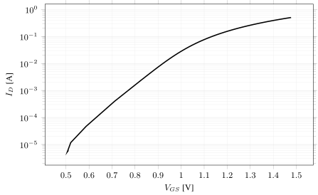
Figure 7: Simulated pass-fet drain current against gate-source voltage for the 500 mA LDO testbench, five decades of current over one volt of gate drive
As such, there are multiple control options for the pass-fet. Below is a summary of a few methods.
We can control the Vgs, or we can switch the number of instances, or we can turn the pass-fet on and off dynamically. What we choose will depend on the application.
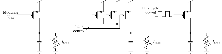
Figure 8: Pass-fet control options: analog Vgs modulation, digital control of parallel instances, and duty-cycle control
Switched Regulators
Linear regulators have poor power efficiency. Linear regulators have the same current in the load, as from the input.
For some applications a poor efficiency might be OK, but for most battery operated systems we’re interested in using the electrons from the battery in the most effective manner.
Another challenge is temperature. A linear regulator with a 5 V input voltage, and 1 V output voltage will have a maximum power efficiency of 20 % (1/5). 80 % of the power is wasted in the pass-fet as heat.
Imagine a LDO driving an 80 W CPU at 1 V from a 5 V power supply. The power drawn from the 5 V supply is 400 W, as such, 320 W would be wasted in the LDO. A quad flat no-leads (QFN) package usually have a thermal resistance of 20 $^{\circ}$C/W, so if it would be possible, the temperature of the LDO would be 6400 $^{\circ}$C. Obviously, that cannot work.
For increased power efficiency, we must use switched regulators.
Imagine a switched regulator with 93 % power efficiency. The power from the 5 V supply would be $80\text{ W}/ 0.93 = 86\text{ W}$, as such, only 6 W is wasted as heat. A temperature increase of $6\text{ W} \times 20\text{ } ^{\circ}\text{C/W} = 120 ^{\circ}$C is still high, but not impossible with a small heat-sink.
All switched regulators are based on devices that store electric field (capacitors), or magnetic field (inductors).
Principles of switched regulators
There is a big difference between the idea for a circuit, and the actual implementation. A real DC/DC implementation may seem overwhelming.
Just look at figure 7 in A 10-MHz 2–800-mA 0.5–1.5-V 90% Peak Efficiency Time-Based Buck Converter With Seamless Transition Between PWM/PFM Modes 4
So before we go into details, let’s have a look at the principles.
Inductive BUCK DC/DC
Below is a common illustration of a inductive DC/DC to step down the voltage.
Imagine Vout is at our desired output voltage, for example 0.8 V. Assume Vin is 1.8 V.
When we close the switch, the inductor will begin to integrate the voltage across the inductor, and the current from Vin to Vout increases.
When we turn off the switch, the inductor current will not stop immediately, it cannot, that’s what
\[V = L \frac{d I}{dt}\]tells us. As a result, the current continues, but now the current is pulled from ground through the diode.
Since we’re pulling current from ground, it should be intuitive that the current from Vin is less than the load current at Vout, assuming Vin > Vout.
The output voltage can be controlled by how long we turn on the switch. Each time we turn on the switch the inductor will inject a charge packet into the load capacitance.
If we have a control loop on the output voltage, then we can get an output voltage that is independent of the input voltage.
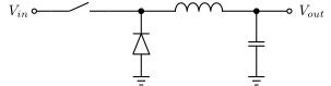
Figure 9: Principle of an inductive buck DC/DC converter: a switch, freewheeling diode, inductor and load capacitor
Capacitive BUCK DC/DC
In a capacitive buck below what we’re doing is charging two capacitors in series to a high voltage, Vin, and then re-configuring the capacitors to be in parallel.
If the capacitors are the same size, then the output voltage would be half the input voltage.
To re-configure the circuit we’d use switches.
A disadvantage with capacitive bucks is that the output voltage is always a factor of the input voltage. When the input voltage changes, the output voltages changes proportionally.
Often we have to insert an LDO after a capacitive buck to make the output voltage independent of input voltage.
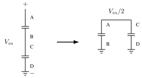
Figure 10: Principle of a capacitive buck: two capacitors charged in series are reconfigured in parallel to halve the voltage
Inductive BOOST DC/DC
Consider the circuit below. Here we setup a current from Vin to ground when the switch is on. When the switch is off push the current through the diode, and thus, the Vout can be higher than Vin.
In a similar manner to the Buck, the output voltage will be impacted by how long we turn on the switch for.
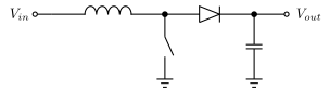
Figure 11: Principle of an inductive boost DC/DC converter: the inductor current is pushed through the diode to an output above Vin
Capacitive BOOST DC/DC
In a capacitive boost we start with a parallel connection, charge the capacitors to Vin, then reconfigure the circuit to a series combination.
As such, the output voltage would be two times the input voltage, assuming the capacitors are equal.
The configuration below is quite often called a “Charge pump”, and can be configured to generate both positive, or negative voltages.
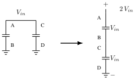
Figure 12: Principle of a capacitive boost (charge pump): two capacitors charged in parallel are stacked in series to double the voltage
Inductive DC/DC converter details
I’ve found that people struggle with inductive DC/DCs. They see a circuit inductors, capacitors, and transistors and think filters, Laplace and steady state. The path of Laplace and steady state will lead you astray and you won’t understand how it works.
Hopefully I can put you on the right path to understanding.
In the figure below we can see a typical inductive switch mode DC/DC converter. The input voltage is $V_{DDH}$, and the output is $V_O$.
Most DC/DCs are feedback systems, so the control will be adjusted to force the output to be what is wanted, however, let’s ignore closed loop for now.
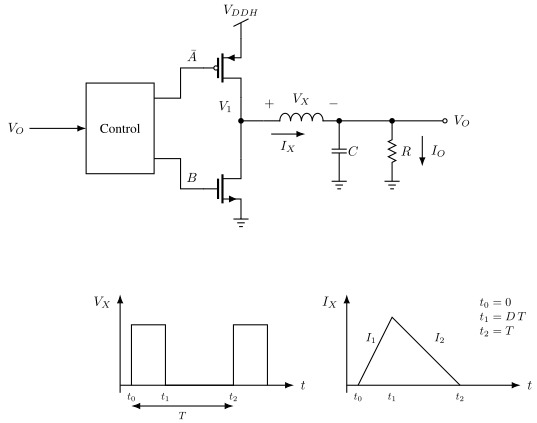
Figure 13: Inductive switch-mode buck converter with control block, and waveforms of the inductor voltage Vx and current Ix
To see what happens I find the best path to understanding is to look at the integral equations.
The current in the inductor is given by
\[I_x(t) = \frac{1}{L} \int{V_x(t) dt}\]and the voltage on the capacitor is given by
\[V_o(t) = \frac{1}{C} \int{(I_x(t) - I_o(t))}dt\]Before you dive into Matlab, Mathcad, Maple, SymPy or another of your favorite math software, it helps to think a bit.
My mathematics is not great, but I don’t think there is any closed form solution to the output voltage of the DC/DC, especially since the state of the NMOS and PMOS is time-dependent.
The output voltage also affect the voltage across the inductor, which affects the current, which affects the output voltage, etc, etc.
The equations can be solved numerically, but a numerical solution to the above integrals needs initial conditions.
There are many versions of the control block, let’s look at two.
Pulse width modulation (PWM)
Assume $I_x=0$ and $I_{o} = 0$ at $t=0$. Assume the output voltage is $V_O=0$. Imagine we set $A=1$ for a fixed time duration. The voltage at $V_1=V_{DDH}$, and $V_x = V_{DDH}-V_O$. As $V_x$ is positive, and roughly constant, the current $I_x$ would increase linearly, as given by the equation of the current above.
Since the $I_x$ is linear, then the increase in $V_o$ would be a second order, as given by the equation of the output voltage above.
Let’s set $A=0$ and $B=1$ for a fixed time duration (it does not need to be the same as duration as we set $A=1$). The voltage across the inductor would be $V_x = 0 - V_o$. The output voltage would not have increased much, so the absolute value of $V_x$ during $A=1$ would be higher than the absolute value of $V_x$ during the first $B=1$.
The $V_x$ is now negative, so the current will decrease, however, since $V_x$ is small, it does not decrease much.
I’ve made a
Jupyter PWM BUCK model - interactive - closed loop with type 3
that numerically solves the equations.
In the figure below we can see how the current during A increases fast, while during B it decreases little. The output voltage increases similarly to a second order function.
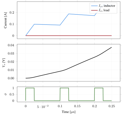
Figure 14: Start-up of the PWM buck model: the inductor current Ix increases fast during A=1, while the output voltage vo grows like a second order function
If we run the simulation longer, see plot below, the DC/DC will start to settle into a steady state condition.
On the top we can see the current $I_x$ and $I_o$, the second plot you can see the output voltage. Turns out that the output voltage will be
\[V_o = V_{in} \times \text{ Duty-Cycle}\], where the duty-cycle is the ratio between the duration of $A=1$ and $B=1$.
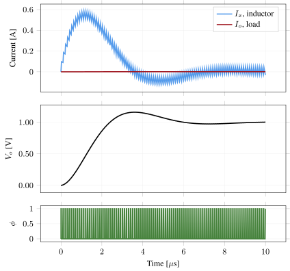
Figure 15: PWM buck model over a longer time: inductor and load currents (top), output voltage settling towards steady state (middle), and switch control A (bottom)
Once the system has fully settled, see figure below, we can see the reason for why DC/DC converters are useful.
During $A=1$ the current $I_x$ increases fast, and it’s only during $A=1$ we pull current from $V_{DDH}$. At the start of $A=0$ the current is still positive, which means we pull current from ground. The average current in the inductor is the same as the average current in the load, however, the current from $V_{DDH}$ is lower than the average inductor current, since some of the current comes from ground.
If the DC/DC was 100% efficient, then the current from the 4 V input supply would be 1/4’th of the current delivered to the 1 V output. 100% efficient DC/DC converters violate the laws of nature, so a good one reaches the low nineties under favourable conditions.
The model above manages 67 %, and it is worth understanding why, because the reason is not that the model is bad. Averaged over the settled part of the run it delivers 0.998 mW and draws 1.478 mW, so 0.48 mW is lost. The inductor carries 1 mA of useful DC and 76 mA peak to peak of ripple, which is 21.8 mA RMS, and all of it flows through the 1 $\Omega$ switch resistance. That is $I_{rms}^2R = 0.477$ mW — within half a percent of the entire loss.
So the whole of the inefficiency here is ripple current heating the switches, and none of that current ever reaches the load. Two things follow. A converter is efficient at the load it was designed for and poor at a much lighter one, because the ripple does not shrink when the load does. And the way to fix it is a bigger inductor or a faster clock, both of which reduce the ripple, and both of which cost something else — area for the first, switching loss for the second. That trade is what the rest of this chapter is about.
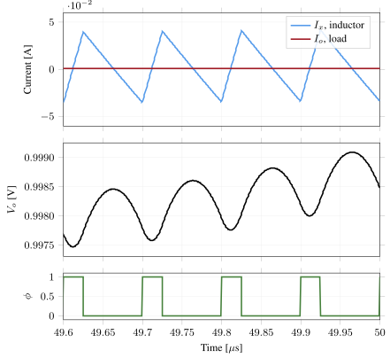
Figure 16: PWM buck model in steady state. The inductor current swings 76 mA peak to peak to supply a 1 mA load, and the output capacitor turns that into 1.6 mV of ripple on a 998 mV output
Real world use
DC/DC converters are used when power efficiency is important. Below is a screenshot of the hardware description in the nRF5340 Product Specification.
We can see 3 inductor/capacitor pairs. One for the “VDDH”, and two for “DECRF” and “DECD”, as such, we can make a good guess there are three DC/DC converters inside the nRF5340.
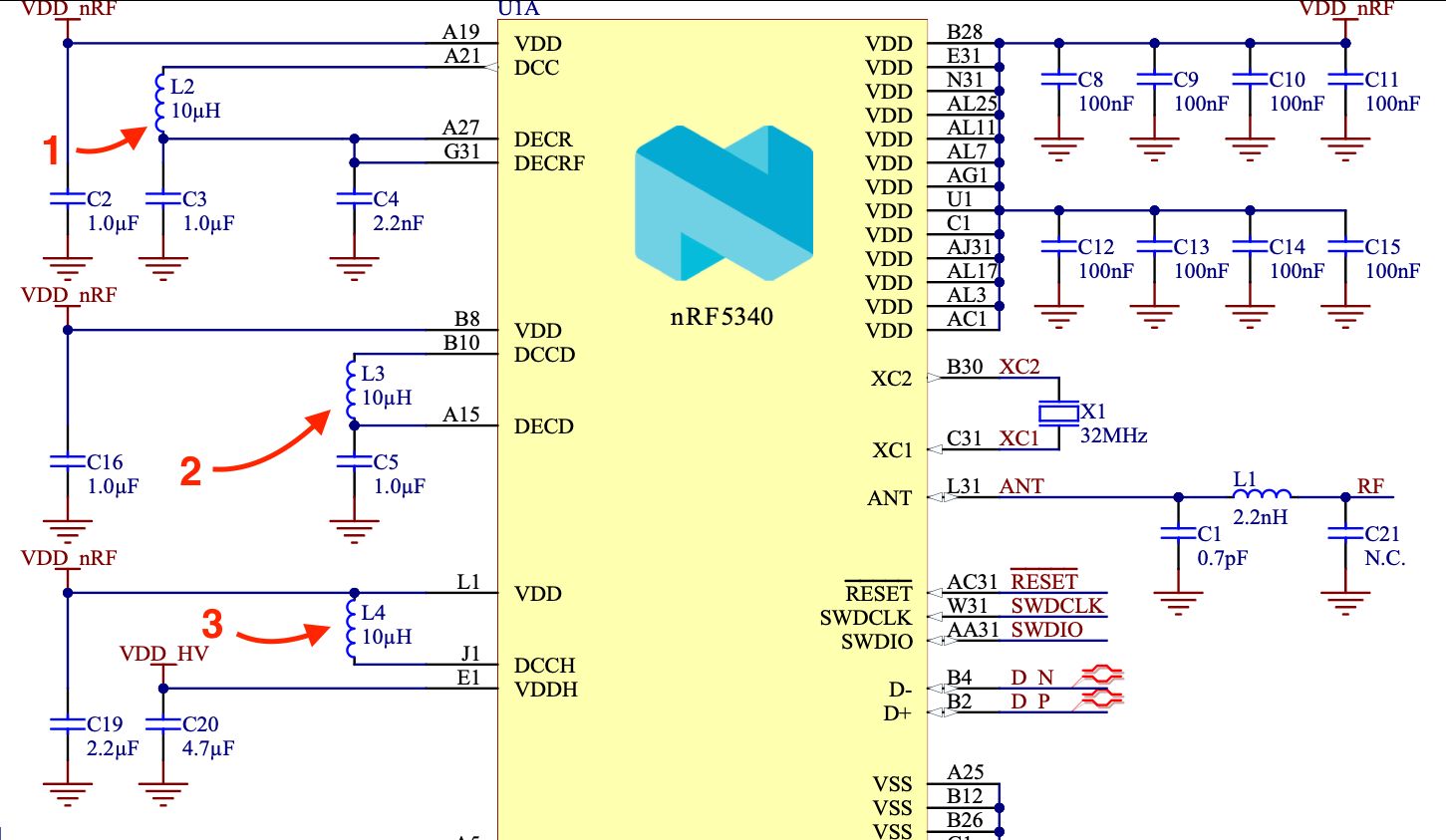
Figure 17: nRF5340 application schematic with three inductor/capacitor pairs, revealing three internal DC/DC converters. Source: Nordic Semiconductor, nRF5340 Product Specification
Pulsed Frequency Mode (PFM)
Power efficiency is key in DC/DC converters. For high loads, PWM, as explained above, is usually the most efficient and practical. For lighter loads, other configurations can be more efficient.
In PWM we continuously switch the NMOS and PMOS, as such, the parasitic capacitance on the $V_1$ node is charged and discharged, consuming power. If the load is close to 0 A, then the parasitic losses can be significant.
In pulsed-frequency mode we switch the NMOS and PMOS when it’s needed. If there is no load, there is no switching, and $V_1$ or $DCC$ in figure below is high impedance.
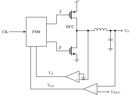
Figure 18: PFM buck architecture with an FSM driving the switches, a zero-cross comparator, and an output voltage comparator
Imagine $V_o$ is at 1 V, and we apply a constant output load. According to the integral equations the $V_o$ would decrease linearly.
In the figure above we observe $V_o$ with a comparator that sets $V_{OL}$ high if the $V_o < V_{REF}$. The output from the comparator could be the inputs to a finite state machine (FSM).
Consider the FSM below. On $vol=1$ we transition to “UP” state where we turn on the PMOS for a fixed number of clock cycles. The inductor current would increase linearly. From the “UP” state we go to the “DWN” state, where we turn on the NMOS. The inductor current would decrease roughly linearly.
The “zero-cross” comparator observes the voltage across the NMOS drain/source. As soon as we turn the NMOS on the current direction in the inductor is still from $DCC$ to $V_o$. Since the current is pulled from ground, the $DCC$ must be below ground. As the current in the inductor decreases, the voltage across the NMOS will at some point be equal to zero, at which point the inductor current is zero.
When $vz=1$ happens in the state diagram, or the zero cross comparator triggers, we transition from the “DWN” state back to “IDLE”. Now the FSM wait for the next time $V_o < V_{REF}$.
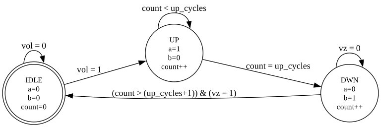
Figure 19: Finite state machine for PFM control with IDLE, UP, and DWN states
I think the name “pulsed-frequency mode” refers to the fact that the frequency changes according to load current, however, I’m not sure of the origin of the name. The name is not important. What’s important is that you understand that mode 1 (PWM) and mode 2 (PFM) are two different “operation modes” of a DC/DC converter.
I made a jupyter model for the PFM mode. I would encourage you to play with them.
Below you can see a period of the PFM buck. The state can be seen in the bottom plot, the voltage in the middle and the current in the inductor and load in the top plot.
Jupyter PFM BUCK model - interactive
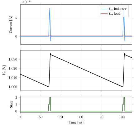
Figure 20: One period of the PFM buck model: inductor and load currents (top), output voltage (middle), and FSM state (bottom)
Summary
The one-page version of this chapter:
- Supply planning comes first: which blocks share a regulator, what noise they inject, what sequence they wake in
- A PMOS pass linear regulator gives the lowest dropout but a hard loop (output pole moves with load); the NMOS follower is easy to stabilize but costs a V_GS of headroom
- Linear regulators burn (V_in - V_out)/V_in of the power - fine for quiet rails, ruinous for big steps
- Inductive DC/DC converters move charge through an inductor at ~90% efficiency: PWM at heavy load, PFM pulses at light load
- Line/load regulation and PSRR are the datasheet numbers; the transient response to a load step is what the digital core actually feels
Would you like to know more?
Search terms: regulator, buck converter, dc/dc converter, boost converter
Linear regulators
A Scalable High-Current High-Accuracy Dual-Loop Four-Phase Switching LDO for Microprocessors 5 Overview of fancy LDO schemes, digital as well as analog
Development of Single-Transistor-Control LDO Based on Flipped Voltage Follower for SoC 6 In capacitor less LDOs a flipped voltage follower is a common circuit, worth a read.
A 200-mA Digital Low Drop-Out Regulator With Coarse-Fine Dual Loop in Mobile Application Processor 7 Some insights into large power systems.
DC-DC converters
Design Techniques for Fully Integrated Switched-Capacitor DC-DC Converters 8 Goes through design of SC DC-DC converters. Good place to start to learn the trade-offs, and the circuits.
High Frequency Buck Converter Design Using Time-Based Control Techniques 9 I love papers that challenge “this is the way”. Why should we design analog feedback loops for our bucks, why not design digital feedback loops?
Single-Inductor Multi-Output (SIMO) DC-DC Converters With High Light-Load Efficiency and Minimized Cross-Regulation for Portable Devices 10 Maybe you have many supplies you want to drive, but you don’t want to have many inductors. SIMO is then an option
A 10-MHz 2–800-mA 0.5–1.5-V 90% Peak Efficiency Time-Based Buck Converter With Seamless Transition Between PWM/PFM Modes 4 Has some lovely illustrations of PFM and PWM and the trade-offs between those two modes.
A monolithic current-mode CMOS DC-DC converter with on-chip current-sensing technique 11 In bucks converters there are two “religious” camps. One hail to “voltage mode” control loop, another hail to “current mode” control loops. It’s good to read about both and make up your own mind.
-
L. L. Lewyn and T. Ytterdal and C. Wulff and K. Martin, Analog Circuit Design in Nanoscale CMOS Technologies 2009 https://doi.org/10.1109/JPROC.2009.2024663 ↩
-
H.-S.-P. Wong and H.-Y. Lee and S. Yu and Y.-S. Chen and Y. Wu and P.-S. Chen and B. Lee and F. T. Chen and M.-J. Tsai, Metal–Oxide RRAM 2012 https://doi.org/10.1109/JPROC.2012.2190369 ↩
-
T. Grasser and B. Kaczer and P. Hehenberger and W. Gos and R. O’Connor and H. Reisinger and W. Gustin and C. Schlunder, Simultaneous Extraction of Recoverable and Permanent Components Contributing to Bias-Temperature Instability 2007 https://doi.org/10.1109/IEDM.2007.4419069 ↩
-
S. J. Kim and W.-S. Choi and R. Pilawa-Podgurski and P. K. Hanumolu, A 10-MHz 2–800-mA 0.5–1.5-V 90% Peak Efficiency Time-Based Buck Converter With Seamless Transition Between PWM/PFM Modes 2018 https://doi.org/10.1109/JSSC.2017.2776298 ↩ ↩2
-
X. Mao and Y. Lu and R. P. Martins, A Scalable High-Current High-Accuracy Dual-Loop Four-Phase Switching LDO for Microprocessors 2022 https://doi.org/10.1109/JSSC.2021.3129620 ↩
-
T. Y. Man and K. N. Leung and C. Y. Leung and P. K. T. Mok and M. Chan, Development of Single-Transistor-Control LDO Based on Flipped Voltage Follower for SoC 2008 https://doi.org/10.1109/TCSI.2008.916568 ↩
-
Y.-J. Lee and W. Qu and S. Singh and D.-Y. Kim and K.-H. Kim and S.-H. Kim and J.-J. Park and G.-H. Cho, A 200-mA Digital Low Drop-Out Regulator With Coarse-Fine Dual Loop in Mobile Application Processor 2017 https://doi.org/10.1109/JSSC.2016.2614308 ↩
-
H.-P. Le and S. R. Sanders and E. Alon, Design Techniques for Fully Integrated Switched-Capacitor DC-DC Converters 2011 https://doi.org/10.1109/JSSC.2011.2159054 ↩
-
S. J. Kim and Q. Khan and M. Talegaonkar and A. Elshazly and A. Rao and N. Griesert and G. Winter and W. McIntyre and P. K. Hanumolu, High Frequency Buck Converter Design Using Time-Based Control Techniques 2015 https://doi.org/10.1109/JSSC.2014.2378216 ↩
-
M.-H. Huang and K.-H. Chen, Single-Inductor Multi-Output (SIMO) DC-DC Converters With High Light-Load Efficiency and Minimized Cross-Regulation for Portable Devices 2009 https://doi.org/10.1109/JSSC.2009.2014726 ↩
-
C. F. Lee and P. Mok, A monolithic current-mode CMOS DC-DC converter with on-chip current-sensing technique 2004 https://doi.org/10.1109/JSSC.2003.820870 ↩