Table of contents
Keywords: Quantization, OSR, NEG FB, STF, NTF, SAR, First Order, SC SD, CT SD, INCR, FOM
ADC state-of-the-art
The performance of an analog-to-digital converter is determined by the effective number of bits (ENOB), the power consumption, and the maximum bandwidth. The effective number of bits contain information on the linearity of the ADC. The power consumption shows how efficient the ADC is. The maximum bandwidth limits what signals we can sample and reconstruct in digital domain.
Many years ago, Robert Walden did a study of ADCs, it is worth looking up the plots.
1999, R. Walden: Analog-to-digital converter survey and analysis 1
There are obvious trends, the faster an ADC is, the less precise the ADC is ( lower SNDR). There are also fundamental limits, Heisenberg tells us that a 20-bit 10 GS/s ADC is impossible, according to Walden.
The plot itself is Figure 4 of that paper, and it is worth looking up: effective bits against sample rate for every converter Walden could find, with four sloped lines drawn over the cloud for the limits set by thermal noise, aperture uncertainty, comparator ambiguity and, at the top, the “Heisenberg” bound. The shape of the cloud is the point. It runs down and to the right, so every decade of sample rate costs somewhere around a bit, and no converter sits above the lines.
Murmann’s survey, two figures further on, plots the same thing with twenty-five more years of data, so you can see both what has changed and what has not.
The uncertainty principle states that the precision we can determine position and the momentum of a particle is \(\sigma_x \sigma_p \ge \frac{\hbar}{2}\). There is a similar relation of energy and time, given by \(\Delta E \Delta t > \frac{h}{2 \pi}\) where $\Delta E$ is the difference in energy, and $\Delta t$ is the difference in time.
You should take these limits with a grain of salt. The plot assumes 50 Ohm and 1 V full-scale. As a result, the “Heisenberg” line that appears to be unbreakable certainly is breakable. Just change the voltage to 100 V, and the number of bits can be much higher. Always check the assumptions.
A more recent survey of ADCs comes from Boris Murmann. He still maintains a list of the best ADCs from ISSCC and VLSI Symposium.
B. Murmann, ADC Performance Survey 1997-2023
A common figure of merit for low-to-medium resolution ADCs is the Walden figure of merit, defined as
\[FOM_W = \frac{P}{2^{ENOB} f_s}\]Below 10 fJ/conv.step is good.
Below 1 fJ/conv.step is extreme.
In the plot below you can see the ISSCC and VLSI ADCs.
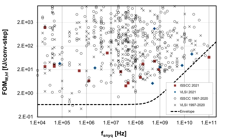
Figure 1: Murmann ADC survey: Walden figure of merit versus Nyquist sample rate for ISSCC and VLSI Symposium ADCs, with the best-in-class envelope
What makes a state-of-the-art ADC
People from NTNU have made some of the world’s best ADCs
If you ever want to make an ADC, and you want to publish the measurements, then you must be better than most. A good algorithm for state-of-the-art ADC design is to first pick a sample rate with low number of data (blank spaces in the plot above), then read the papers in the vicinity of the blank space to understand the application, then set a target FOM which is best in world, then try and find an ADC architecture that can achieve that FOM.
That’s pretty much the algorithm I, and others, have followed to make state-of-the-art ADCs. A few of the NTNU ADCs are:
[1] A Compiled 9-bit 20-MS/s 3.5-fJ/conv.step SAR ADC in 28-nm FDSOI for Bluetooth Low Energy Receivers 2
[2] A 68 dB SNDR Compiled Noise-Shaping SAR ADC With On-Chip CDAC Calibration
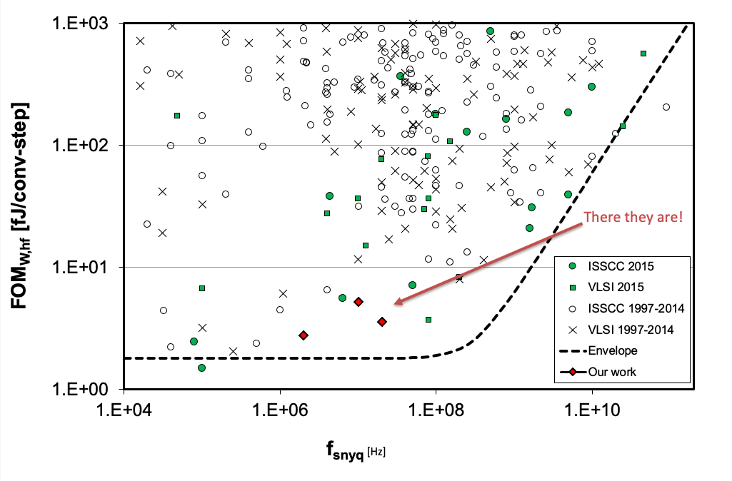
Figure 2: Walden figure of merit versus Nyquist sample rate with the NTNU compiled SAR ADCs marked as “Our work” near the envelope
In order to publish, there must be something new. Preferably a new circuit. Below is the circuit from [1]. It’s a standard successive-approximation register (SAR) analog-to-digital converter.
The differential input signal is sampled on a capacitor array where the bottom plate is connected to either VSS or VREF. Once the voltage is sampled, the comparator will decide whether the differential voltage is larger, or smaller than 0. Depending on the decision, the MSB capacitors (left-most) in figure will switch the bottom plate in order to effectively subtract a voltage equivalent to half the VREF voltage.
The comparator makes another decision, and 1/4’th the VREF voltage is subtracted or added. Then 1/8’th and so on implementing a binary search to find the input voltage.
The “bit-cycling” (binary-search) loop is self-timed, as such, when the comparator has made a decision, the next cycle starts.
In (b) we can see the enable flip-flop for the next stage. The CK bar is the sample clock, as such, A is high during sampling. The output of the comparator (P and N) is low.
As soon as the comparator makes a decision, P or N goes high, A will be pulled low, if EI is enabled.
In (c) we can see that the bottom plate of the capacitors $D_{P0}$, $D_{P1}$, $D_{N0}$, and $D_{N1}$, are controlled by P and N.
In (d) we can see that the bottom plate of the capacitors also used to set the comparator clock low again (CO), resetting the comparator, and pulling P and N low, which in (b) enables the next SAR logic state.
How fast the $D_{XX}$ settle depend on the size of the capacitors, as such, the comparator clock will be slow for the MSB, and very fast for the LSB. This was my main circuit contribution in the paper. I think it’s quite clever, because both the VDD and the capacitor corner will change the settling time. It’s important that the capacitor values fully settle before the next comparator decision, and as a result of the circuit in (c,d) the delay is automatically adjusted.
For further details see the paper.
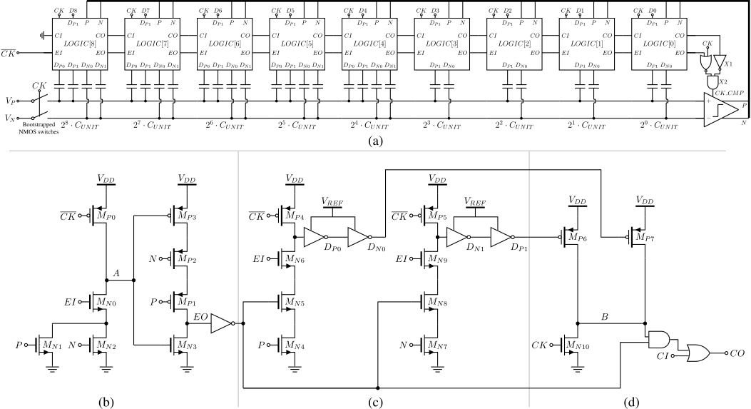
Figure 3: SAR ADC schematic: (a) capacitor array with self-timed SAR logic chain and comparator, (b) enable flip-flop, (c) bottom-plate switching of the CDAC, (d) comparator clock generation
For state-of-the-art ADC papers it’s not sufficient with the idea, and simulation. There must be proof that it actually works. No-one will really believe that the ADC works until there is measurements of an actual taped out IC.
Below you can see the layout of the IC I made for the paper. Notice that there are 9 ADCs. I had many ideas that I wanted to try out, and I was not sure what would actually be state of the art. As a result, I taped out multiple ADCs.
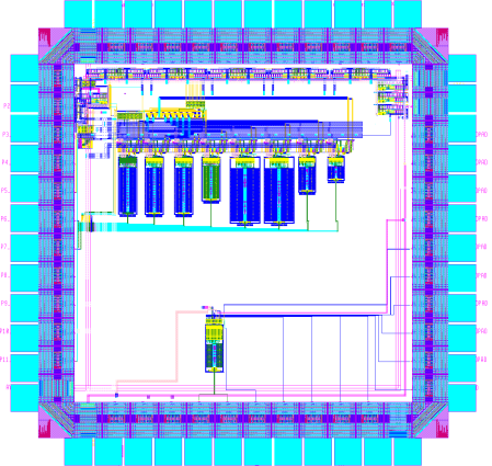
Figure 4: Layout of the test chip with nine ADC variants inside the pad ring
The two ADCs that I ended up using in the paper are shown below. The one on the left was made with 180 nm IO transistors, while the one on the right was made with core-transistors. Notice that the layout of the two is quite similar.
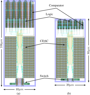
Figure 5: Layout of the two compiled SAR ADCs with comparator, logic, CDAC and switch: (a) 180 nm IO-transistor version (40 x 106 um), (b) core-transistor version (39 x 80 um)
Once taped out, and many months of waiting, a few months of measurement in the lab, I had some results that would be good enough to qualify for the best conference, and luckily the best journal.
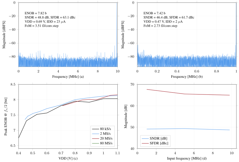
Figure 6: Measured performance of the core-transistor ADC: (a, b) output spectra at 0.69 V and 0.47 V supply, (c) peak ENOB versus VDD, (d) SNDR and SFDR versus input frequency
Comparing my ADCs to others, we can see that the FOM is similar to others. Based on the FOM it might not be clear why the paper was considered state-of-the-art.
The circuit technique mentioned above would not have been enough to qualify. The big thing was the “Compiled” line. Compared to the other “Compiled” mine was 300 times better, and on par with other state-of-the-art.
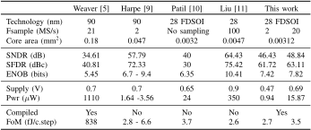
Figure 7: Comparison table against state-of-the-art SAR ADCs, where “This work” stands out as the only compiled ADC with competitive figure of merit
The big thing was how I made the ADC. I started with a definition of a transistor, as shown below
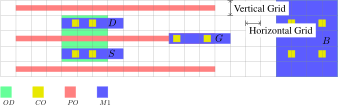
Figure 8: Transistor definition used by the layout compiler: diffusion (OD), contacts (CO), poly (PO) and metal 1 (M1) placed on a vertical and horizontal grid
And then wrote a compiler (in Perl, later C++ ciccreator) to compile a object definition file, a SPICE netlist and a technology rule file into the full ADC layout.
In (a) you can see one of the cells in the SAR logic, (b) is the spice file, and (c) is the definition of the routing. The numbers to the right in the routing creates the paths shown in (d).
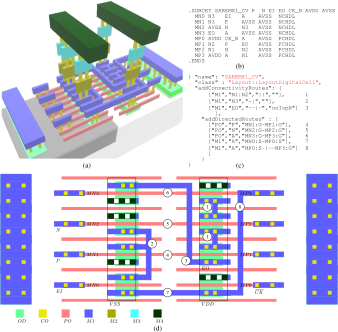
Figure 9: Compiled SAR logic cell: (a) 3D view of the layout, (b) SPICE netlist, (c) object definition with routing rules, (d) the resulting routed layout
The implementation is the SPICE netlist, and the object definition file (JSON) and the rule file.
What I really like is the fact that the compilation could generate GDSII or SKILL, or these days, Xschem schematics and Magic layout.
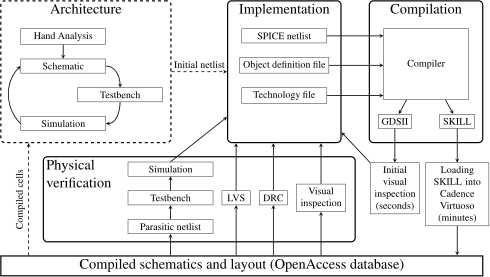
Figure 10: Compiled ADC design flow: architecture, implementation files (SPICE netlist, object definition, technology file), compilation to GDSII or SKILL, and physical verification
The cool thing with a compiled ADC is that it’s easy to port between technologies. Since the original ADC, I’ve ported the ADC to multiple closed PDKs (22 nm FDSOI, 22 nm, 28 nm, 55 nm, 65 nm and 130nm). In the summer of 2022 I made an open source port to skywater 130nm.
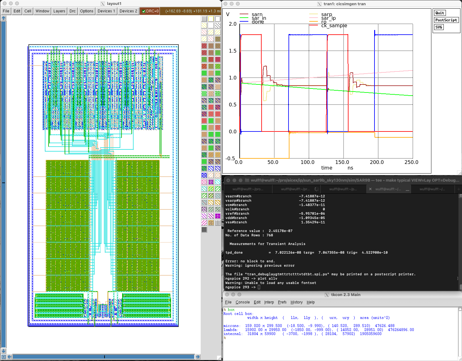
Figure 11: The SAR ADC ported to skywater 130 nm: Magic layout of the ADC core and ngspice transient simulation of a conversion
One of my Ph.D students built on-top on my work, and made a noise-shaped compiled SAR ADC, shown below, more on that later.
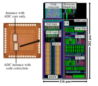
Figure 12: Noise-shaping compiled SAR ADC: die photo of the two ADC instances and the 116 um x 202 um core layout with CDAC, SAR logic, loop filter, OTAs and code correction
High resolution FOM
For high-resolution ADCs, it’s more common to use the Schreier figure of merit, which can also be found in
B. Murmann, ADC Performance Survey 1997-2022 (ISSCC & VLSI Symposium)
The Walden figure of merit assumes that thermal noise does not constrain the power consumption of the ADC, which is usually true for low-to-medium resolution ADCs. To keep the Walden FOM you can double the power for a one-bit increase in ENOB. If the ADC is limited by thermal noise, however, then you must quadruple the capacitance (reduce $kT/C$ noise power) for each 1-bit ENOB increase. Accordingly, the power must also go up four times.
For higher resolution ADC the power consumption is set by thermal noise, and the Schreier FOM allows for a 4x power consumption increase for each added bit.
\[FOM_S = SNDR + 10\log\left(\frac{f_s/2}{P}\right)\]Above 180 dB is extreme
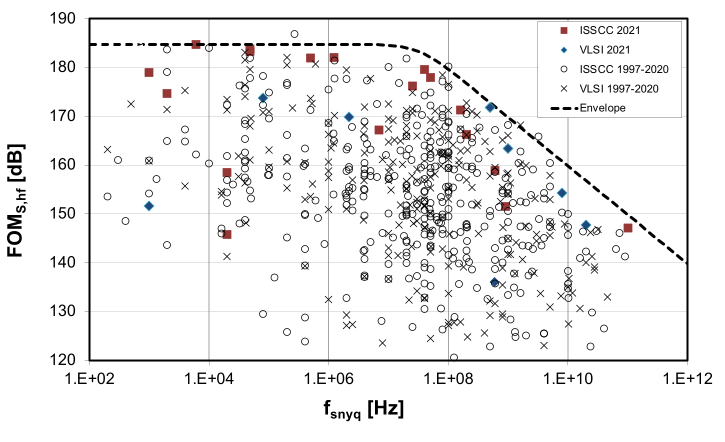
Figure 13: Murmann ADC survey: Schreier figure of merit versus Nyquist sample rate, where the envelope flattens around 185 dB for thermal-noise limited ADCs
Quantization
Sampling turns continuous time into discrete time. Quantization turns continuous value into discrete value. Any complete ADC is always a combination of sampling and quantization.
In our mathematical drawings of quantization we often define $y[n]$ as the output, the quantized signal, and $x[n]$ as the discrete time, continuous value input, and we add some “noise”, or “quantization noise” $e[n]$, where $x[n] = y[n] - e[n]$.
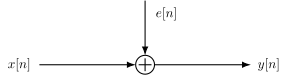
Figure 14: Linear model of quantization: the quantization noise e[n] is added to the input x[n] to form the output y[n]
Maybe you’ve even heard the phrase “Quantization noise is white” or “Quantization noise is a random Gaussian process”?
I’m here to tell you that you’ve been lied to. Quantization noise is not white, nor is it a Gaussian process. Those that have lied to you may say “yes, sure, but for high number of bits it can be considered white noise”. I would say that’s similar to saying “when you look at the earth from the moon, the surface looks pretty smooth without bumps, so let’s say the earth is smooth with no mountains”.
I would claim that it’s an unnecessary simplification. It’s obvious to most that the earth would appear smooth from really far away, but they would not be surprised by Mount Everest, since they know it’s not smooth. An Alien that has been told that the earth is smooth, would be surprised to see Mount Everest.
But if Quantization noise is not white, what is it?
The figure below shows the input signal x and the quantized signal y.
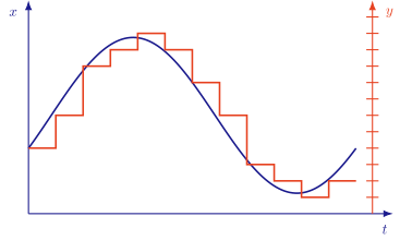
Figure 15: A continuous time sinusoid input x (blue) and the quantized output y (red)
To see the quantization noise, first take a look at the sample and held version of $x$ in green in the figure below. The difference between the green ($x$ at time n) and the red ($y$) would be our quantization noise $e$
The quantization noise is contained between $+\frac{1}{2}$ Least Significant Bit (LSB) and $-\frac{1}{2}$ LSB.
This noise does not look random to me, but I can’t see what it is, and I’m pretty sure I would not be able to work it out either.
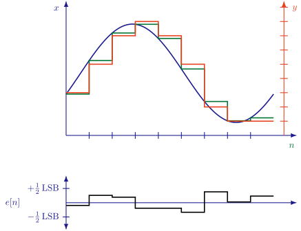
Figure 16: Sample-and-held input (green), quantized output (red), and the resulting quantization error e[n], bounded by plus/minus half an LSB
Luckily, there are people in this world that love mathematics, and that can delve into the details and figure out what $e[n]$ is. A guy called Blachman wrote a paper back in 1985 on quantization noise.
See The intermodulation and distortion due to quantization of sinusoids 3 for details
In short, the quantizer output for a sinusoidal input is an exact harmonic series,
\[y(t) = \sum_{p=1}^\infty{A_p\sin{p\omega t}}\]and the quantization noise is what is left when the input is taken back out,
\[e_n(t) = y(t) - A\sin{\omega t}\]which is the same series with the $\delta_{p1}A$ term removed. It is worth keeping the two apart. The series below carries the fundamental at nearly full amplitude, so it is emphatically not something with zero mean and variance $\Delta^2/12$; the difference is.
where p is the harmonic index, and
\[A_p = \begin{cases} \delta_{p1}A + \sum_{m = 1}^\infty{\frac{2}{m\pi}J_p(2m\pi A)} &, p = \text{ odd} \\ 0 &, p = \text{ even} \end{cases}\] \[\delta_{p1} \begin{cases} 1 &, p=1 \\ 0 &, p \neq 1 \end{cases}\]and \(J_p(x)\) is a Bessel function of the first kind, A is the amplitude of the input signal.
If we approximate the amplitude of the input signal as
\[A = \frac{2^n - 1}{2} \approx 2^{n-1}\]where n is the number of bits, we can rewrite as
\[y(t) = \sum_{p=1}^\infty{A_p\sin{p\omega t}}\] \[A_p = \delta_{p1}2^{n-1} + \sum_{m=1}^\infty{\frac{2}{m\pi}J_p(2m\pi 2^{n-1})}, p=odd\]Obvious, right?
I must admit, it’s not obvious to me. But I do understand the implications. The quantization noise is an infinite sum of input signal odd harmonics, where the amplitude of the harmonics is determined by a sum of a Bessel function.
A Bessel function of the first kind looks like this
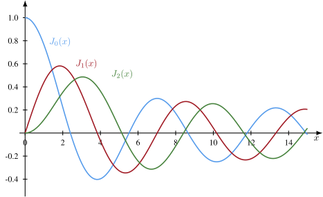
Figure 17: Bessel functions of the first kind, J0(x), J1(x) and J2(x), showing the oscillatory behavior that shapes the quantization noise harmonics
So I would expect the amplitude to show signs of oscillatory behavior for the harmonics. That’s the important thing to remember. The quantization noise is odd harmonics of the input signal
The mean value is zero
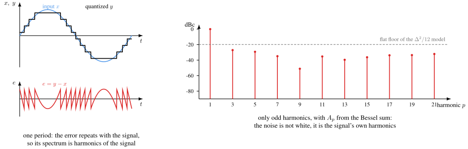
Figure 18: What the Bessel series actually says: a sine through a 3-bit quantizer, the error it leaves, and the odd harmonic amplitudes $A_p$ from the formula above, against the flat floor the $\Delta^2/12$ model would predict
Here is the formula drawn out. On the left, a sine through a three bit quantizer, and underneath it the error it leaves behind. The error is not random: it repeats exactly once per signal period, which is the whole reason its spectrum can only contain harmonics of the signal.
On the right, the amplitudes $A_p$ evaluated from the Bessel sum. They agree with a direct FFT of the quantized sine to about a tenth of a percent, so this is not an approximation of the noise, it is the noise. Compare the spikes with the dashed line, which is where the $\Delta^2/12$ white noise model would put a flat floor: the total power is the same, but the distribution is nothing like it.
If you want to feel this rather than read it, the interactive version puts the bit count on a slider. Walk it up and watch the harmonics fall and crowd together, until somewhere around eight bits calling them a noise floor finally becomes fair.
Watch the rate they fall at, because it is not the 6 dB per bit you might expect. An individual harmonic drops about 9 dB per bit, tending to $30\log 2 = 9.03$ dB. The 6 dB per bit belongs to the total quantization noise power, and the difference between the two is the whole reason the noise floor idea works at all: each harmonic falls 9 dB, but the number of harmonics crammed below $f_s/2$ doubles, which adds 3 dB back. Nine down, three up, six net. So as you add bits the spectrum does not merely shrink, it redistributes — fewer and fewer dB in each of more and more spikes, until no individual spike is worth naming and the aggregate is all that is left.
\[\overline{e_n(t)} = 0\]and variance (mean square, since mean is zero), or noise power, can be approximated as
\[\overline{e_n(t)^2} = \frac{\Delta^2}{12}\]Signal to Quantization noise ratio
Assume we wanted to figure out the resolution, or effective number of bits for an ADC limited by quantization noise. A power ratio, like signal-to-quantization noise ratio (SQNR) is one way to represent resolution.
Take the signal power, and divide by the noise power
\[SQNR = 10 \log\left(\frac{A^2/2}{\Delta^2/12}\right) = 10 \log\left(\frac{6 A^2}{\Delta^2}\right)\] \[\Delta = \frac{2A}{2^B}\] \[SQNR = 10 \log\left(\frac{6 A^2}{4 A^2/2^{2B}}\right) = 20 B \log 2 + 10 \log 6/4\] \[SQNR \approx 6.02 B + 1.76\]You may have seen the last equation before, now you know where it comes from.
Understanding quantization
Below I’ve tried to visualize the quantization process q.py, which also exists as an interactive page where the number of bits is a slider and the SQNR is measured for you.
The left most plot is a sinusoid signal and random Gaussian noise. The signal is not a continuous time signal, since that’s not possible on a digital computer, but it’s an approximation.
The plots are FFTs of a sinusoidal signal combined with noise. These are complex FFTs, so they show both negative and positive frequencies; the x-axis is normalized to each record’s sample rate, from $-f_s/2$ to $+f_s/2$. When the text below talks about bins, multiply $f/f_s$ by the record length (2048 after sampling) to get the bin number. Notice that there are two spikes, which should not be surprising, since a sinusoidal signal is a combination of two frequencies.
\[sin(x) = \frac{e^{ix} - e^{-ix}}{2i}\]The second plot from the left is after sampling, notice that the noise level increases. The rise is exactly $10\log(4) = 6.02$ dB, and it is worth being careful about why, because there are two tempting explanations and they are not two effects to be added together.
Both are named in the same expression. With a Hann window and the peak normalisation that freqDomain uses, the noise floor per bin relative to the tone is
where $\sigma$ is the time-domain noise and $M$ the record length. The record length is right there in the denominator, so a four times shorter record does raise the floor 6 dB. But $\sigma^2$ is in the numerator, and whether it survives decimation is exactly the folding question. Decimating without an anti-alias filter preserves the total noise power, $\sigma$ does not change, and the floor rises the full 6 dB. Put an ideal brick-wall filter in front and $\sigma^2$ drops by four as well, the two effects cancel term for term, and the floor does not move at all.
So the answer is 6.02 dB in total and the two mechanisms must not be added: they are two ways of booking the same rise, and the experiment that separates them is to filter before decimating. It is the first appearance in this chapter of a rule worth keeping — throwing samples away only helps if something band-limits the noise first.
The right plot is after quantization, where I’ve used the function below.
def adc(x,bits):
    levels = 2**bits
    delta = 2/levels
    y = np.floor(x/delta)*delta + delta/2
    return np.clip(y, -1 + delta/2, 1 - delta/2)
A B-bit converter has exactly $2^B$ levels, spaced by $\Delta = 2/2^B$, sitting half a step off zero. The obvious one-liner np.round(x*2**bits)/2**bits looks like a quantizer but is not one: its step is $2^{-B}$, so at one bit it produces five output levels over $\pm 1$ rather than two, and the measured SQNR comes out a whole bit too good. The plots below are a real one bit converter - two levels, one comparator.
I really need you to internalize a few things from the right most plot. Really think through what I’m about to say.
Can you see how the noise (what is not the two spikes) is not white? White noise would be flat in the frequency domain, but the noise is not flat.
Notice also that this is a genuine one bit quantizer: two levels, so the output is a square wave, and what you are looking at is its odd harmonic series - exactly the $A_p$ of the Bessel formula above, folded back into the band wherever a harmonic lands above $f_s/2$.
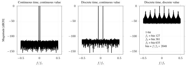
Figure 19: FFT of a sinusoid with noise as continuous value (left), after sampling (middle), and after 1-bit quantization (right), where the quantization noise shows up as distinct harmonic spikes rather than a white noise floor
If you run the python script you can zoom in and check the highest spikes. A 1-bit quantizer is a sign detector, so its output for a sine input is a square wave, and a square wave has only odd harmonics with amplitudes falling as $1/p$. That is exactly what the plot shows. The fundamental is at bin 127, and the measured spikes are
| harmonic | $20\log(1/p)$ | measured | bin |
|---|---|---|---|
| 3 | $-9.54$ dB | $-9.54$ dB | 381 |
| 5 | $-13.98$ dB | $-13.98$ dB | 635 |
| 7 | $-16.90$ dB | $-16.90$ dB | 889 |
| 9 | $-19.08$ dB | $-19.08$ dB | 905 |
| 11 | $-20.83$ dB | $-20.83$ dB | 651 |
Agreement to the second decimal with a formula you can write down from memory is a good afternoon’s work. But look at the last two rows. The ninth harmonic should be at $9 \times 127 = 1143$ and the eleventh at $11 \times 127 = 1397$, and neither bin exists — the record is only 2048 points, so anything above 1024 is above half the sample rate. They fold: $2048 - 1143 = 905$ and $2048 - 1397 = 651$. The harmonics march monotonically down in amplitude, but from bin 889 onwards they march backwards along the frequency axis, which is why a spectrum plot of an aliased converter can look like nonsense until you work out which harmonic each spike really is.
This is worth internalising, because in a real converter you do not get to compare against a formula. A spike at 651 with nothing at 1397 is not evidence of some mysterious distortion mechanism; it is the eleventh harmonic, folded. If you change the python script to reduce the frequency, fdivide=2**9, and increase number of points, N=2**16, as in the plot below, the eleventh harmonic no longer folds, and you’ll see it directly at bin 1397.
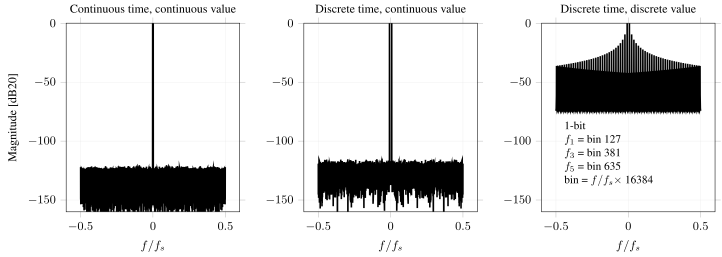
Figure 20: The same 1-bit quantization with lower input frequency and a 16384-point FFT, where the 11th harmonic appears directly at bin 1397 instead of folding
All the other spikes are the odd harmonics above the sample rate that fold. The infinite sum of harmonics will fold, some in-phase, some out of phase, depending on the sign of the Bessel function.
From the function for the amplitude of the quantization noise for harmonic indices higher than $p=1$
\[A_p = \sum_{m=1}^\infty{\frac{2}{m\pi}J_p(2m\pi 2^{n-1} ) }\text{, p=odd}\]we can see that the input to the Bessel function increases faster for a higher number of bits $n$. As such, from the Bessel function figure above, I would expect that the sum of the Bessel function is a lower value. Accordingly, the quantization noise reduces at higher number of bits.
A consequence is that the quantization noise becomes more and more uniform, as can be seen from the plot of a 10-bit quantizer below. That’s why people say “Quantization noise is white”, because for a high number of bits, it looks white in the FFT.
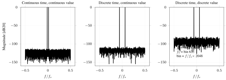
Figure 21: FFT of the same signal with a 10-bit quantizer, where the quantization noise is closer to uniform and looks almost white
Why you should care about quantization noise
So why should you care whether the quantization noise looks white, or actually is white? A class of ADCs called oversampling and sigma-delta modulators rely on the assumption that quantization noise is white. In other words, the cross-correlation between noise components at different time points is zero. As such the noise power sums as a sum of variance, and we can increase the signal-to-noise ratio.
We know that assumption to be wrong though, quantization noise is not white. For noise components at harmonic frequencies the cross-correlation will be high. As such, when we design oversampling or sigma-delta based ADC we will include some form of dithering (making quantization noise whiter). For example, before the actual quantizer we inject noise, or we make sure that the thermal noise is high enough to dither the quantizer.
Everybody that thinks that quantization noise is white will design non-functioning (or sub-optimal) oversampling and sigma-delta ADCs. That’s why you should care about the details around quantization noise.
Oversampling
Here is the question this section answers. If the quantizer’s noise is a fixed amount that we cannot reduce, can we win anything by sampling faster than the signal actually demands, and then averaging the extra samples away?
The answer is yes, and the reason is that signal and noise behave differently under summation. A slow signal is nearly the same from one sample to the next, so summing samples adds it up coherently. Noise is not, so it adds up incoherently. Everything below is bookkeeping on that one asymmetry.
Assume a signal $x[n] = a[n] + b[n]$ where $a$ is a sampled sinusoid and $b$ is a random process where cross-correlation is zero for any time except for $n=0$. Assume that we sum two (or more) equally spaced signal components, for example
\[y = x[n] + x[n+1]\]What would the signal to noise ratio be for $y$?
Noise power
Our mathematician friends have looked at this, and as long the noise signal $b$ is random then the noise power for the oversampled signal $b_{osr} = b[n] + b[n+1]$ will be
\[\overline{b_{osr}^2} = OSR \times \overline{b^2}\]where OSR is the oversampling ratio. If we sum two time points the $OSR=2$, if we sum 4 time points the $OSR=4$ and so on.
For fun, let’s go through the mathematics
Define $b_1 = b[n]$ and $b_2 = b[n+1]$ and compute the noise power
\[\overline{(b_1 + b_2)^2} = \overline{b_1^2 + 2b_1b_2 + b_2^2}\]Let’s replace the mean with the actual function
\[\frac{1}{N}\sum_{n=0}^N{\left(b_1^2 + 2b_1b_2 + b_2^2\right)}\]which can be split up into
\[\frac{1}{N}\sum_{n=0}^N{b_1^2} + \frac{1}{N}\sum_{n=0}^N{2b_1b_2} + \frac{1}{N}\sum_{n=0}^N{b_2^2}\]we’ve defined the cross-correlation to be zero, as such
\[\overline{(b_1 + b_2)^2} = \frac{1}{N}\sum_{n=0}^N{b_1^2} + \frac{1}{N}\sum_{n=0}^N{b_2^2} = \overline{b_1^2} + \overline{b_2^2}\]but the noise power of each of the $b$’s must be the same as $b$, so
\[\overline{(b_1 + b_2)^2} = 2\overline{b^2}\]Signal power
For the signal $a$ we need to calculate the increase in signal power as OSR increases.
I like to think about it like this. $a$ is low frequency, as such, samples $n$ and $n+1$ is pretty much the same value. If the sinusoid has an amplitude of 1, then the amplitude would be 2 if we sum two samples. As such, the amplitude must increase with the OSR.
The signal power of a sinusoid is $A^2/2$, accordingly, the signal power of an oversampled signal must be $(OSR \times A)^2/2$.
Signal to Noise Ratio
Take the signal power to the noise power
\[\frac{(OSR \times A)^2/2}{OSR \times \overline{b^2}} = OSR \times \frac{A^2/2}{\overline{b^2}}\]We can see that the signal to noise ratio increases with increased oversampling ratio, as long as the cross-correlation of the noise is zero
Signal to Quantization Noise Ratio
Now put the two halves together. The quantizer always makes the same total amount of noise, $\Delta^2/12$, and always spreads it evenly from zero to $f_s/2$. Sampling faster than we need does not reduce that total, it only spreads it over a wider band, so the part that lands inside the band we actually care about shrinks by the oversampling ratio.
in-band quantization noise for an oversampling ratio (OSR)
\[\overline{e_n(t)^2} =\frac{\Delta^2}{12 OSR}\]That single division by OSR is the whole of oversampling, and everything else in this section is arithmetic on it. Dividing the noise power by OSR multiplies the ratio by OSR:
\[SQNR = 10 \log\left(\frac{6 A^2}{\Delta^2/OSR}\right) = 10 \log\left(\frac{6 A^2}{\Delta^2}\right) + 10 \log(OSR)\] \[SQNR \approx 6.02B + 1.76 + 10 \log(OSR)\]so the SQNR improves by $10\log(2) \approx 3$ dB for an OSR of 2, and $10\log(4) \approx 6$ dB for an OSR of 4 — 3 dB for every doubling.
\[10 \log(2) \approx 3 dB\] \[10 \log(4) \approx 6 dB\]Compare that with the 6.02 dB a real bit is worth and the exchange rate falls out: three decibels is half a bit, so oversampling buys 0.5-bit per doubling of OSR
It is a poor exchange rate, and it is worth feeling how poor before moving on. Going from an 8-bit converter to a 12-bit one by oversampling alone needs $OSR = 2^8 = 256$, which means running the analog front end 256 times faster than the signal requires. That is the wall that noise shaping exists to get around.
Python oversample
There are probably more elegant (and faster) ways of implementing oversampling in python, but I like to write the dumbest code I can, simply because dumb code is easy to understand.
Below you can see an example of oversampling. The oversample function takes in a vector and the OSR. For each index it sums OSR future values.
def oversample(x,OSR):
    N = len(x)
    y = np.zeros(N)

    for n in range(0,N):
        for k in range(0,OSR):
            m = n+k
            if (m < N):
                y[n] += x[m]
    return y
Below we can see the plot for OSR=2, the right most plot is the oversampled version.
The noise has all frequencies, and it’s the high frequency components that start to cancel each other. An average filter (sometimes called a sinc filter due to the shape in the frequency domain) will have zeros at $\pm fs/2$ where the noise power tends towards zero.
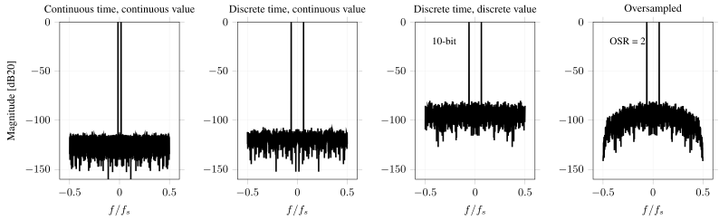
Figure 22: FFTs from continuous value to 10-bit quantized to oversampled with OSR=2 (right), where the averaging filter nulls the noise towards half the sample rate
The low frequency components will add, and we can notice how the noise power increases close to the zero frequency (middle of the x-axis).
For an OSR of 4 we can count four dips in the noise floor, although there are really three nulls: a length-4 moving average has zeros at $f_s/4$, $f_s/2$ and $3f_s/4$, and on this two-sided plot the $f_s/2$ null is split across both edges so you see half of it twice. For OSR=2 there is one null, at $f_s/2$, and it shows up only as the two edges.
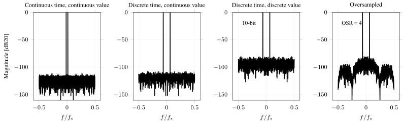
Figure 23: The same FFTs with OSR=4 (right), where the moving-average filter puts three nulls in the noise floor, seen as four dips on this two-sided plot, and the noise power increases close to zero frequency
The code for the plots is osr.py. I would encourage you to play a bit with the code, and make sure you understand oversampling. If you would rather drag a slider than edit a file, the interactive version plots the measured in-band SNR against OSR next to the ideal 3 dB per octave.
Noise Shaping
Look at the OSR=4 plot above, and look at it honestly, because it does not show what you might hope. Near zero frequency the averaged floor is not lower than the unaveraged one — measured from the script it is about 0.8 dB higher for OSR=4, which is the same thing the previous paragraph said when it noted that the low-frequency components add. The averaging filter has done almost nothing to the noise in the band we care about, because that noise is in its passband.
So where is the 6 dB that the theory promised? It is there, but it comes from restricting the band, not from the filter. Integrate the same unaveraged spectrum over $\vert f\vert < f_s/8$ instead of the whole $f_s/2$ and the signal-to-noise ratio improves by close to $10\log(4)$, exactly as the derivation said. The filter’s job is not to create that improvement but to make it safe to collect: it removes the out-of-band noise that would otherwise fold back on top of the signal when you decimate. These plots never decimate, so the payoff is invisible in them. That is a limitation of the figure, not of oversampling.
What the plots do show clearly is the ceiling. Even with the averaging, the noise level of the discrete-time continuous-value plot is much lower than anything the quantized paths achieve.
What if we could do something, add some circuitry, before the quantization such that the quantization noise was reduced?
That’s what noise shaping is all about. Adding circuits such that we can “shape” the quantization noise. We can’t make the quantization noise disappear, or indeed reduce the total noise power of the quantization noise, but we can reduce the quantization noise power for a certain frequency band.
But what circuitry can we add?
The magic of feedback
A generalized feedback system is shown below, it could be a regulator, a unity-gain buffer, or something else.
The output $V_o$ is subtracted from the input $V_i$, and the error $V_x$ is shaped by a filter $H(s)$.
If we make $H(s)$ infinite, then $V_o = V_i$. If you’ve never seen such a circuit, you might ask “Why would we do this? Could we not just use $V_i$ directly?”. There are many reasons for using a circuit like this, let me explain one instance.
Imagine we have a VDD of 1.8 V, and we want to make a 0.9 V voltage for a CPU. The CPU can consume up to 10 mA. One way to make a divide by two circuit is with two equal resistors connected between VDD and ground. We don’t want the resistive divider to consume a large current, so let’s choose 1 MOhm resistors. The current in the resistor divider would then be about 1 $\mu$A. We can’t connect the CPU directly to the resistor divider, the CPU can draw 10 mA. As such, we need a copy of the voltage at the mid-point of the resistor divider that can drive 10 mA.
Do you see now why a circuit like the one below is useful? If not, you should really come talk to me so I can help you understand.
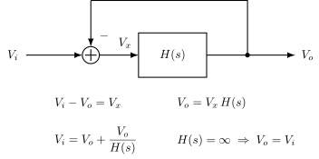
Figure 24: A generalized feedback system where the error between input and output is shaped by a filter H(s), and the output equals the input when H(s) is infinite
Sigma-delta principle
Let’s modify the feedback circuit into the one below. I’ve added an ADC and a DAC to the feedback loop, and the $D_o$ is now the output we’re interested in. The equation for the loop would be
\[D_o = adc\left[H(s)\left(V_i - dac(D_o)\right)\right]\]But how can we now calculate the transfer function $\frac{D_o}{V_i}$? Both $adc$ and $dac$ could be non-linear functions, so we can’t disentangle the equation. Let’s make assumptions.
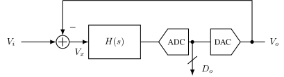
Figure 25: The sigma-delta principle: a feedback loop with a filter H(s), an ADC (quantizer) and a DAC in the feedback path, with digital output Do
The DAC assumption
Assumption 1: the $dac$ is linear, such that $V_o = dac(D_o) = A D_o + B$, where $A$ and $B$ are scalar values.
The DAC must be linear, otherwise our noise-shaping ADC will not work.
One way to force linearity is to use a 1-bit DAC, which has only two points, so should be linear. For example \(V_o = A \times D_o\), where $D_o \in {0,1}$. Even a 1-bit DAC could be non-linear if $A$ is time-variant, so $V_o[n] = A(t)\times D_o[n]$, this could happen if the reference voltage for the DAC changed with time.
I’ve made a couple noise shaping ADCs, and in the first one I made I screwed up the DAC. It turned out that the DAC current had a signal dependent component which lead to a non-linear behavior.
The ADC assumption
Assumption 2: the $adc$ can be modeled as a linear function $D_o = adc(x) = x + e$, where e is white noise source
We’ve talked about this, the $e$ is not white, especially for low-bit ADCs, so we usually have to add noise. Sometimes it’s sufficient with thermal noise, but often it’s necessary to add a random, or pseudo-random noise source at the input of the ADC.
The modified equation
With the assumptions we can change the equation into
\[D_o = adc\left[H(s)\left(V_i - dac(D_o)\right)\right] = H(s)\left( V_i - A D_o\right) + e\]In noise-shaping texts it’s common to write the above equation as
\[y = H(s)(u - y) + e\]or in the sample domain
\[y[n] = e[n] + h*(u[n] - y[n])\]which could be drawn in a signal flow graph as below.
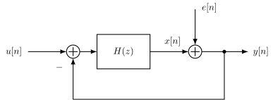
Figure 26: Signal flow graph of the noise-shaping loop: the difference between input u[n] and output y[n] is filtered by H(z) and the quantization noise e[n] is added at the quantizer
in the Z-domain the equation would turn into
\[Y(z) = E(z) + H(z)\left[U(z) - Y(z)\right]\]The whole point of this exercise was to somehow shape the quantization noise, and we’re almost at the point, but to show how it works we need to look at the transfer function for the signal $U$ and for the noise $E$.
Signal transfer function
Assume U and E are uncorrelated, and E is zero
\[Y = HU - HY\] \[STF = \frac{Y}{U} = \frac{H}{1 + H} = \frac{1}{1 + \frac{1}{H}}\]Imagine what will happen if H is infinite. Then the signal transfer function (STF) is 1, and the output $Y$ is equal to our input $U$. That’s exactly what we wanted from the feedback circuit.
Noise transfer function
Assume U is zero
\[Y = E - HY \rightarrow NTF = \frac{1}{1 + H}\]Imagine again what happens when H is infinite. In this case the noise-transfer function becomes zero. In other words, there is no added noise.
Combined transfer function
In the combined transfer function below, if we make $H(z)$ infinite, then $Y = U$ and there is no added quantization noise. I don’t know how to make $H(z)$ infinite everywhere, so we have to choose at what frequencies it’s “infinite”.
\[Y(z) = STF(z) U(z) + NTF(z) E(z)\]There are a large set of different $H(z)$ and I’m sure engineers will invent new ones. We usually classify the filters based on the number of zeros in the NTF, for example, first-order (one zero), second order (two zeros) etc. There are books written about sigma-delta modulators, and I would encourage you to read those to get a deeper understanding. I would start with Delta-Sigma Data Converters: Theory, Design, and Simulation.
First-Order Noise-Shaping
We want an infinite $H(z)$. One way to get an infinite function is an accumulator, for example
\[y[n+1] = x[n] + y[n]\]or in the Z-domain
\[zY = X + Y \rightarrow Y(z-1) = X\]which has the transfer function
\[H(z) = \frac{1}{z-1}\]The signal transfer function is
\[STF = \frac{1/(z-1)}{1 + 1/(z-1)} = \frac{1}{z} = z^{-1}\]and the noise transfer function
\[NTF = \frac{1}{1 + 1/(z-1)} = \frac{z-1}{z} = 1 - z^{-1}\]In order calculate the Signal to Quantization Noise Ratio we need to have an expression for how the NTF above filters the quantization noise.
In the book they replace the $z$ by the Laplace variable and then walk out onto the imaginary axis, $s = j\omega$, which is where a transfer function turns into a frequency response.
\[z = e^{sT} \;\underset{s=j\omega}{\longrightarrow}\; e^{j\omega T} = e^{j2 \pi f/f_s}\]inserted into the NTF we get the function below. The three lines are one trick applied once, so it is worth knowing what you are looking for before reading them. We want $1 - e^{-j\theta}$ turned into something whose magnitude we can read off, and the only identity available is $\sin\theta = (e^{j\theta}-e^{-j\theta})/2j$. So we factor out half the exponent, $e^{-j\pi f/f_s}$, which leaves a difference of two conjugate exponentials in the bracket — exactly the shape of that identity — and then divide and multiply by $2j$ to make it literally a sine. Everything pulled out has magnitude 1, so it contributes phase and nothing else.
\[\begin{aligned} NTF(f) &= 1- e^{-j2 \pi f/f_s} \\ &= \frac{e^{j \pi f/f_s} -e^{-j \pi f/f_s}}{2j}\times 2j \times e^{-j\pi f/f_s} \\ &= \sin\left(\frac{\pi f}{f_s}\right) \times 2j \times e^{-j \pi f/f_s} \end{aligned}\]The arithmetic magic is really to extract the $2j \times e^{-j \pi f/f_s}$ from the first expression such that the initial part can be translated into a sinusoid.
When we take the absolute value to figure out how the NTF changes with frequency the complex parts disappears (equal to 1)
\[\vert NTF(f)\vert = \left\vert 2 \sin\left(\frac{\pi f}{f_s}\right)\right\vert\]The signal power for a sinusoid is
\[P_s = A^2/2\]The in-band noise power for the shaped quantization noise is
\[P_n = \int_{-f_0}^{f_0} \frac{\Delta^2}{12}\frac{1}{f_s}\left[2 \sin\left(\frac{\pi f}{f_s}\right)\right]^2 df\]The integral is not actually tedious, and it is worth doing once because it explains both of the odd-looking constants in the answer. In band, $f$ is much smaller than $f_s$, so $\sin(\pi f/f_s) \approx \pi f/f_s$ and the integrand becomes a parabola:
\[P_n \approx \frac{\Delta^2}{12}\frac{1}{f_s}\frac{4\pi^2}{f_s^2}\int_{-f_0}^{f_0} f^2 df = \frac{\Delta^2}{12}\frac{4\pi^2}{f_s^3}\frac{2f_0^3}{3}\]That $f_0^3$ is where the whole advantage comes from. Ordinary oversampling had the in-band noise falling as $f_0$; here it falls as $f_0^3$, because the shaping makes the noise density itself proportional to $f^2$. Substituting $OSR = f_s/2f_0$:
\[P_n \approx \frac{\Delta^2}{12}\frac{\pi^2}{3}\frac{1}{OSR^3}\]The $OSR^3$ becomes the $30\log(OSR)$ — three times the $10\log(OSR)$ of plain oversampling — and the $\pi^2/3$ becomes the penalty $10\log(\pi^2/3) = 5.17$ dB. Take the ratio to $P_s = A^2/2$ and
\[SQNR = 6.02 B + 1.76 - 5.17 + 30 \log(OSR)\]If we compare to pure oversampling, where the SQNR improves by $10 \log(OSR)$, a first order sigma-delta improves by $30 \log(OSR)$. That’s a significant improvement.
SQNR and ENOB
Below is the signal-to-quantization noise ratio’s for Nyquist up to second order sigma-delta. Read them as one family. Every line starts from the same $6.02B + 1.76$, and each step down the list buys a steeper dependence on OSR at the cost of a larger fixed penalty.
The second-order line follows from repeating the derivation above with $NTF = (1-z^{-1})^2$, so the noise density goes as $f^4$ instead of $f^2$. The integral then produces $OSR^5$, hence $50\log(OSR)$, and $\pi^4/5$ in place of $\pi^2/3$, hence $10\log(\pi^4/5) = 12.9$ dB. The pattern continues: an $L$’th order modulator gives $(20L+10)\log(OSR)$ and a penalty of $10\log(\pi^{2L}/(2L+1))$.
The penalties are real, and at low OSR they can outweigh the steeper slope. Setting the first- and second-order expressions equal gives a crossover at $OSR \approx 2.4$: below that, second-order shaping is worse than first-order, because the extra 7.7 dB of penalty has not yet been earned back by the extra $20\log(OSR)$. Higher order is not automatically better, it is better eventually, and where “eventually” starts is a number you can compute before committing to an architecture.
\[SQNR_{nyquist} \approx 6.02B + 1.76\] \[SQNR_{oversample} \approx 6.02B + 1.76 + 10 \log(OSR)\] \[SQNR_{\Sigma\Delta 1} \approx 6.02 B + 1.76 - 5.17 + 30 \log(OSR)\] \[SQNR_{\Sigma\Delta 2} \approx 6.02 B + 1.76 - 12.9 + 50 \log(OSR)\]We could compute an effective number of bits, as shown below.
\[ENOB = (SQNR - 1.76)/6.02\]Assume 1-bit quantizer, what would be the maximum ENOB?
| OSR | Oversampling | First-order | Second-order |
|---|---|---|---|
| 4 | 2.0 | 3.1 | 3.9 |
| 64 | 4.0 | 9.1 | 13.9 |
| 1024 | 6.0 | 15.1 | 23.9 |
Table: ENOB of a 1-bit quantizer ($B = 1$), from the three expressions above.
Read down a column and you see what oversampling buys you; read across a row and you see what an architecture buys you. Plain oversampling is hopeless: a thousand-fold increase in sample rate turns one bit into six. First-order shaping turns the same thousand-fold into fifteen, and second-order into twenty-four. That is the entire argument for building the loop, and it is why a 1-bit modulator followed by a decimation filter is a sensible way to make a 20-bit converter, while a 1-bit oversampled ADC is not a way to make anything.
The second-order column also shows the crossover discussed above. At $OSR=4$ second-order leads first-order by less than a bit, because the extra 7.7 dB penalty has barely been paid off; by $OSR=1024$ it leads by nine.
Examples
Python noise-shaping
I want to demystify noise-shaping modulators. I think one way to do that is to show some code. You can find the code at sd_1st.py, and an interactive version that runs the same loop in your browser and decodes the bitstream back into the input.
Below we can see an excerpt. Again pretty stupid code, and I’m sure it’s possible to make a faster version (for loops in python are notoriously slow).
For each sample in the input vector $u$ I compute the input to the quantizer $x$, which is the sum of the previous input to the quantizer and the difference between the current input and the previous output $y_{sd}$.
The quantizer generates the next $y_{sd}$ and I have the option to add dither.
Three details in the full script are not in this excerpt and matter if you want to reproduce the plots. The input is scaled to 0.7 of full scale, because a true 1-bit loop overloads if you drive it all the way — the integrator runs away and the output degenerates into a slow square wave. The first two samples are thrown away, because the integrator starts at zero and needs a moment to settle. And the dither amplitude is a quarter of a quantizer step, which is enough to break up idle tones without swamping the signal.
One inconsistency is worth flagging rather than hiding. This quantize uses a step of $2/(2^B-1)$ for more than one bit, a mid-tread converter whose levels include zero, while the adc function earlier in this chapter uses $\Delta = 2/2^B$, a mid-rise converter with no zero level. Both are real converters and both appear in real silicon; they differ by half a step and by whether a zero input produces a zero output. The $\Delta^2/12$ result holds for either. Just do not mix the two definitions when you are comparing measured numbers against theory, which is exactly the sort of half-LSB discrepancy that costs an afternoon.
def quantize(v,bits):
    #- 2**bits levels reaching +/-1, so bits=1 is
    #- a genuine two-level quantizer
    levels = 2**bits
    if(levels == 2):
        return 1.0 if v >= 0 else -1.0
    step = 2/(levels-1)
    return float(np.clip(np.round(v/step)*step,-1,1))

# u is discrete time, continuous value input
M = len(u)
y_sd = np.zeros(M)
x = np.zeros(M)
for n in range(1,M):
    x[n] = x[n-1] + (u[n]-y_sd[n-1])
    y_sd[n] = quantize(x[n]
        + dither*np.random.randn()/(4*2**bits),bits)
The right-most plot is the one with noise-shaping. We can observe that the noise seems to tend towards zero at zero frequency, as we would expect. The accumulator above would have an infinite gain at infinite time (it’s the sum of all previous values), as such, the NTF goes towards zero at 0 frequency.
If we look at the noise we can also see the non-white quantization noise, which will degrade our performance. I hope by now, you’ve grown tired of me harping on the point that quantization noise is not white
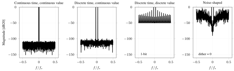
Figure 27: First-order sigma-delta modulator with 1-bit quantizer and no dither, where the noise-shaped spectrum (right) tends towards zero at zero frequency but contains distinct tones
In the figure below I’ve turned on dither, and we can see how the noise looks “better”, which I know is not a qualitative statement, but ask anyone that’s done 1-bit quantizers. It’s important to have enough random noise.
Be clear about what has been bought and what has been paid, though, because the y-axis of the plot tells both halves of the story. The distinct tones are gone and the floor is smooth, which is what “better” means here: a smooth floor is predictable, it does not move when the input does, and it will not land a spur in the middle of your signal band on a Tuesday. But the floor is also higher, and the notch at zero frequency is shallower. Running the loop with and without dither, the in-band signal-to-noise ratio drops by a decibel or two. Dither is not free noise reduction; it converts a small amount of signal-to-noise ratio into a large amount of predictability. That is usually a good trade for a 1-bit quantizer with a slow input, where the alternative is idle tones parked wherever the input DC level happens to put them, and a bad trade for a many-bit quantizer that was never going to produce tones in the first place.
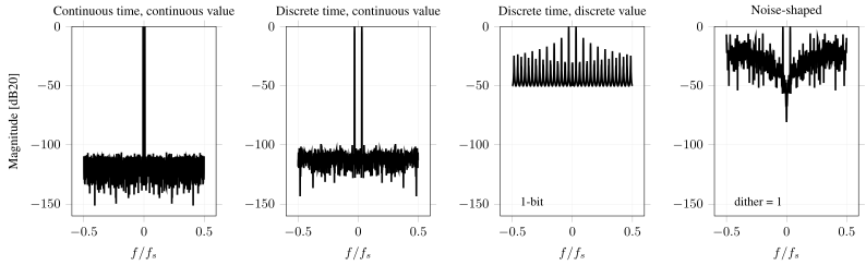
Figure 28: The same first-order 1-bit sigma-delta modulator with dither enabled, where the noise-shaped spectrum (right) is smoother and more noise-like
In papers it’s common to use a logarithmic frequency axis, as shown below. In the plot I only show the positive frequencies of the FFT. From the shape of the quantization noise we can also see the first order behavior, as a straight 20 dB per decade rise, which is much easier to read off a log axis than off the linear ones above.
Two things have changed from the previous two figures, and it is worth saying so rather than letting you wonder. The quantizer here is 5-bit, not 1-bit, so the floor is far lower and there are no idle tones to speak of. And the y-axis is a magnitude spectrum in dB, not a power spectral density: nothing has been normalised to the bin width, so the absolute level is only meaningful relative to the tone.
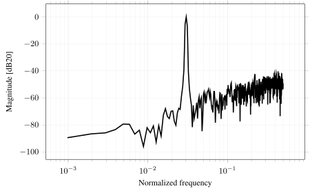
Figure 29: Magnitude spectrum of the output of a 5-bit first-order sigma-delta modulator on a logarithmic frequency axis, showing the 20 dB/decade shaping of the quantization noise
The wonderful world of SD modulators
Open-Loop Sigma-Delta
On my Ph.D I did some work on
Resonators in Open-Loop Sigma-Delta Modulators 4
which was a pure theoretical work. The idea was to use modulo integrators (local control of integrator output swing) in front of large latency multi-bit quantizers to achieve a high SNR.
The plot below shows a fifth order NTF where there are two complex conjugate zero pairs, and a zero at zero frequency. With a higher order filter one can use a lower OSR, and still achieve high ENOB.
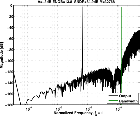
Figure 30: Output spectrum of an open-loop sigma-delta modulator with a fifth-order NTF (two complex conjugate zero pairs and a zero at DC), reaching 13.8 bit ENOB and 84.9 dB SNDR
Noise Shaped SAR
One of my Ph.d students made a
A 68 dB SNDR Compiled Noise-Shaping SAR ADC With On-Chip CDAC Calibration 5
In a SAR ADC, once the bit-cycling is complete, the analog value on the capacitors is the actual quantization error. That error can be fed to a loop filter, H(z), and amplified in the next conversion, accordingly a combination of SAR and noise-shaping.
In the paper the SD modulator was also used to calibrate the non-linearity in the CDAC, as the MSB capacitor won’t be exactly N times larger than the smallest capacitor.
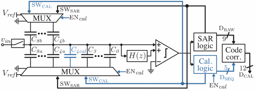
Figure 31: Architecture of the noise-shaping SAR ADC: capacitive DAC with multiplexers, loop filter H(z), integrating comparator, SAR logic, calibration logic and code correction
The loop filter was a switched cap loop filter, and we can see the NTF below. The first OTA made use of chopping to reduce the offset.
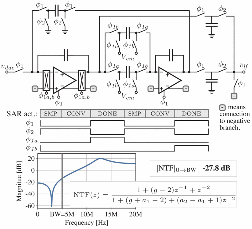
Figure 32: The switched-capacitor loop filter with two OTAs (the first one chopped), the clock phases relative to the SAR activity, and the resulting NTF with -27.8 dB in-band suppression
Control-Bounded ADCs
One of my current Ph.D students is working on an even more advanced type of sigma-delta ADC. Actually, it’s more a super-set of SD ADCs called control-bounded ADCs.
Design Considerations for a Low-Power Control-Bounded A/D Converter
A block diagram of a Leapfrog ADC version of a control-bounded ADC is shown below.
Here we’re walking into advanced maths territory, but to simplify, I think it’s correct to say that a control-bounded ADC seeks to control the local analog state, $x_n(t)$ such that no voltage is saturated. The digital control signals $s_n(t)$ are used to infer the state of the input $u(t)$ using a form of Bayesian Statistics.
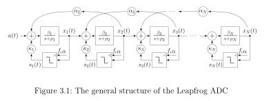
Figure 33: Block diagram of the Leapfrog control-bounded ADC: a chain of continuous-time integrators with local digital control loops s(t) that keep the analog states x(t) bounded
Below we can see a power spectral density plot of the ADC, and we can observe how the quantization noise is shaped. I think it’s a third order NTF with a zero at zero frequency and a complex conjugate zero pair, a notch, at 8 MHzish.
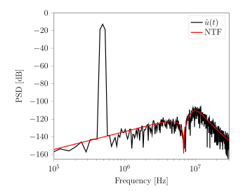
Figure 34: Power spectral density of the control-bounded ADC’s estimated input together with the NTF, a third-order shaping with a notch around 8 MHz
Complex Sigma-Delta
There are cool sigma-delta modulators with crazy configurations and that may look like an exercise in “Let’s make something complex”, however, most of them have a reasonable application. One example is the one below for radio receivers
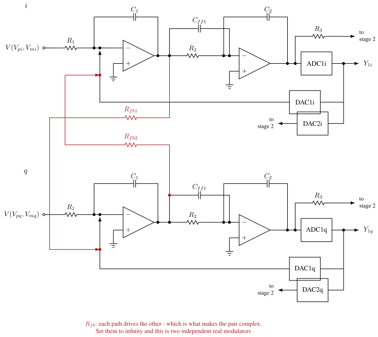
Figure 35: One stage of the quadrature modulator, with the second cascaded stage and the differential wiring left out. Inspired by Breems et al. 6
The cross-coupling in red is the whole of what makes it quadrature. Take it away and there are two independent real modulators, each with a noise transfer function that is symmetric about zero frequency, because a real circuit cannot tell $+f$ from $-f$. Put it back and the pair responds to a rotating phasor rather than an oscillating one, so the notch can sit on one side of zero and not the other. That is exactly what a near zero-IF receiver wants: the wanted channel is a little above zero, its image a little below, and only a complex modulator can quieten one without quietening both.
My first Sigma-Delta
The first sigma-delta modulator I made in “real-life” was similar to the one shown below.
The input voltage is translated into a current, and the current is integrated on capacitor $C$. The $R_{offset}$ is to change the mid-level voltage, while $R_{ref}$ is the 1-bit feedback DAC. The comparator is the quantizer. When the clock strikes the comparator compares the $V_o$ and $V_{ref}/2$ and outputs a 1-bit digital output $D$
The complete ADC is operated in a “incremental mode”, which is a fancy way of saying
Reset your sigma-delta modulator, run the sigma delta modulator for a fixed number of cycles (i.e 1024), and count the number of ones at $D$
The effect of an “incremental mode” is to combine the modulator and a output filter so the ADC appears to be a slow Nyquist ADC.
For more information, ask me, or see the patent at Analogue-to-digital converter
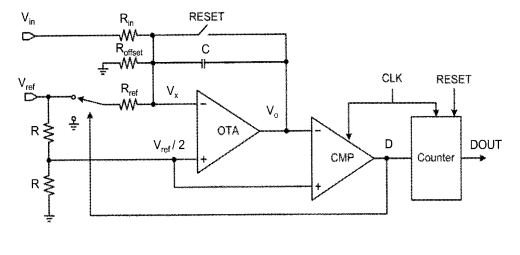
Figure 36: Incremental first-order sigma-delta ADC from the patent: input and reference resistors into an OTA integrating on C, a clocked comparator as quantizer, and a counter as output filter
Summary
The one-page version of this chapter:
- One number for an ADC: the figure of merit - Walden for speed-limited, Schreier for noise-limited designs
- Ideal quantization gives SQNR = 6.02 N + 1.76 dB, and the white-noise model of it holds only for busy inputs
- Oversampling spreads the same noise power over more bandwidth: 3 dB (half a bit) per octave
- Feedback around the quantizer shapes the noise away from the band: first-order sigma-delta buys 9 dB per octave, and higher order buys more
- The decimation filter is where the promised resolution is actually cashed out
- A compiled ADC is a netlist, an object file and a rule file - portable across processes in weeks, and good enough for JSSC
Would you like to know more?
The design of sigma-delta modulation analog-to-digital converters 7
Delta-sigma modulation in fractional-N frequency synthesis 8
A CMOS Temperature Sensor With a Voltage-Calibrated Inaccuracy of ± 0.15 C (3sigma) From -55 Cto 125 C 9
A 20-mW 640-MHz CMOS Continuous-Time Sigma-Delta ADC With 20-MHz Signal Bandwidth, 80-dB Dynamic Range and 12-bit ENOB 10
A Micro-Power Two-Step Incremental Analog-to-Digital Converter 11
-
Robert H. Walden, Analog to Digital Converter Survey and Analysis 1999 https://doi.org/10.1109/49.761034 ; ↩
-
Wulff, Carsten and Ytterdal, Trond, A Compiled 9-bit 20-MS/s 3.5-fJ/conv.step SAR ADC in 28-nm FDSOI for Bluetooth Low Energy Receivers 2017 https://doi.org/10.1109/JSSC.2017.2685463 ↩
-
N. Blachman, The intermodulation and distortion due to quantization of sinusoids 1985 https://doi.org/10.1109/TASSP.1985.1164729 ↩
-
C. Wulff and T. Ytterdal, Resonators in Open-Loop Sigma–Delta Modulators 2009 https://doi.org/10.1109/TCSI.2009.2015211 ↩
-
Garvik, Harald and Wulff, Carsten and Ytterdal, Trond, A 68 dB SNDR Compiled Noise-Shaping SAR ADC With On-Chip CDAC Calibration 2019 https://doi.org/10.1109/A-SSCC47793.2019.9056925 ↩
-
L. J. Breems and R. Rutten and R. H. M. van Veldhoven and G. van der Weide, A 56 mW Continuous-Time Quadrature Cascaded $\Sigma\Delta$ Modulator With 77 dB DR in a Near Zero-IF 20 MHz Band 2007 https://doi.org/10.1109/JSSC.2007.908765 ↩
-
B. Boser and B. Wooley, The design of sigma-delta modulation analog-to-digital converters 1988 https://doi.org/10.1109/4.90025 ↩
-
T. Riley and M. Copeland and T. Kwasniewski, Delta-sigma modulation in fractional-N frequency synthesis 1993 https://doi.org/10.1109/4.229400 ↩
-
K. Souri and Y. Chae and K. A. A. Makinwa, A CMOS Temperature Sensor With a Voltage-Calibrated Inaccuracy of $\pm$ 0.15$ ^\circ$ C (3$\sigma$ ) From $-$ 55$^\circ$ C to 125$^\circ$ C 2013 https://doi.org/10.1109/JSSC.2012.2214831 ↩
-
G. Mitteregger and C. Ebner and S. Mechnig and T. Blon and C. Holuigue and E. Romani, A 20-mW 640-MHz CMOS Continuous-Time $\Sigma\Delta$ ADC With 20-MHz Signal Bandwidth, 80-dB Dynamic Range and 12-bit ENOB 2006 https://doi.org/10.1109/JSSC.2006.884332 ↩
-
C.-H. Chen and Y. Zhang and T. He and P. Y. Chiang and G. C. Temes, A Micro-Power Two-Step Incremental Analog-to-Digital Converter 2015 https://doi.org/10.1109/JSSC.2015.2413842 ↩