Table of contents
Keywords: OTA, Headroom, Five Transistor, Current Mirror OTA, Two-Stage, Miller Compensation, Folded Cascode, Inverter-Based, Nauta, CMFB, Bias, Op Amp, Dynamic Amplifiers, Verification
OTAs
An operational transconductance amplifier (OTA) takes a differential voltage in and pushes a current out. Load it with a capacitor and it integrates; wrap feedback around it and it becomes whatever the feedback network says - a switched capacitor integrator, a filter, an ADC residue amplifier, a regulator error amplifier. Almost every analog system in this book has an OTA somewhere inside it.
The idea is old: the name and the first commercial part arrived in 1969, when Wheatley and Wittlinger argued that the OTA obsoletes the op amp 1, and the OTA-based filter tradition that grew from it is summarized in Geiger and Sanchez-Sinencio’s tutorial 2.
This chapter walks through the OTA topologies that still make sense in nanoscale CMOS, where the supply is around 0.8 V. That last constraint is the important one: half the classic topologies in the textbooks were invented for 5 V, and do not survive the trip down.
The headroom budget
Start with the arithmetic that kills topologies. At $V_{DD}$ = 0.8 V, with a threshold voltage around 0.4 V:
\[V_{DD} = 0.8 \text{ V}, V_{t} \approx 0.4\text{ V}\]One gate-source voltage
\[V_{GS} \approx 0.5 \text{ V}\]One saturated current source, one cascode
\[V_{DSAT} \approx 0.1 \text{ V each}\]Stack of two gate-source voltages? Dead.
Telescopic cascode with swing? Dead.
A gate-source voltage plus a tail current source plus a load already sums to about 0.7 V, so the five transistor OTA barely fits. Add a cascode on both sides and the output can still move a little. Stack two gate-source voltages - a telescopic cascode with wide swing, a folded mirror with source degeneration - and there is nothing left.
The consequences run through the whole chapter: we get gain from long transistors and from more stages, not from stacking; we bias at moderate or weak inversion, where $V_{GS}$ is low and $g_m/I_D$ is high; and every volt of output swing has to be argued for.
Five transistor OTA
The five transistor OTA in Figure 1 is the differential pair from the circuits chapter with its loads folded into a current mirror: the mirror takes the left branch current, flips it over, and slams it into the right branch, so the full differential current reaches the single ended output.
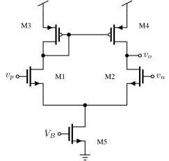
Figure 1: Five transistor OTA
\[A = g_{m1} (r_{ds2} \parallel r_{ds4})\] \[\omega_{ugf} = \frac{g_{m1}}{C_L}\]Output swing: \(V_{DD} - 2 V_{DSAT}\)
The gain is one intrinsic gain - 20 to 40 dB in a nanoscale process - and the unity gain frequency is set by the input pair transconductance over the load capacitance. The swing is generous: only a $V_{DSAT}$ lost at each rail.
For a buffer, a modest filter, or a bias loop, this is the correct answer, and reaching for anything fancier is vanity. When it is not enough, it is for one of two reasons: not enough gain, or not enough drive - and the two failures point to two different upgrades.
Current mirror OTA
If the problem is drive - a big load capacitor and a tail current that cannot slew it - the current mirror OTA in Figure 2 helps. Both branch currents are mirrored outwards with a gain $K$, and the output branch can source and sink $K$ times the tail current.
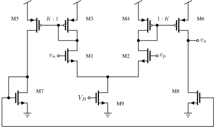
Figure 2: Current mirror OTA with mirror ratio $K$
\[A = K g_{m1} (r_{ds6} \parallel r_{ds8})\] \[\omega_{ugf} = \frac{K g_{m1}}{C_L}\]Slew rate: \(\pm K I_{tail} / C_L\)
The price is the extra mirror pole - the diode connected loads and their mirror partners add a pole at roughly $g_{m3}/C_{mirror}$, which eats phase margin as $K$ grows - and the noise and offset of four more transistors. $K$ of 2 to 5 is typical. All transistors sit one $V_{GS}$ or one $V_{DSAT}$ from a rail, so the topology is fully at home at 0.8 V, which is why it is everywhere in low voltage design.
Two stage (Miller) OTA
If the problem is gain, add a stage. The two stage OTA in Figure 3 puts a common source stage after the five transistor OTA: two intrinsic gains multiplied, and the output stage swings to within one $V_{DSAT}$ of each rail - the best swing any OTA can offer, which matters when the supply is 0.8 V and every millivolt of signal range counts.
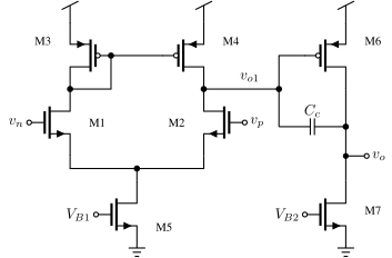
Figure 3: Two stage OTA with Miller compensation
\[A = g_{m1}(r_{ds2} \parallel r_{ds4}) \times g_{m6}(r_{ds6} \parallel r_{ds7})\] \[\omega_{ugf} = \frac{g_{m1}}{C_c}\]Pole splitting: dominant pole down, output pole out to \(\approx \frac{g_{m6}}{C_L}\)
Two stages means two poles, and two poles in a feedback loop must be pushed apart. That is the Miller capacitor $C_c$’s job: it is $C_{gd}$ multiplied by the second stage gain, on purpose - the Miller effect from the MOSFET chapter, hired instead of feared. The input pole drops, the output pole rises to about $g_{m6}/C_L$, and the amplifier crosses unity at $g_{m1}/C_c$ with the second pole safely beyond.
The famous flaw: $C_c$ also feeds the input signal forward past the second stage, creating a right half plane zero at $g_{m6}/C_c$ that steals phase. The standard fix is a resistor in series with $C_c$, which moves the zero to infinity - or on top of the second pole, if you are feeling precise.
The subtler flaw is the supply rejection. Above the dominant pole, $C_c$ effectively shorts the output to the first stage output, which turns M6 into a diode connected device seen from the loop - and M6’s source sits on $V_{DD}$. High frequency supply ripple therefore walks through the output stage with close to unity gain, exactly where the loop gain is already too small to fight it. Of the topologies in this chapter, the two stage Miller OTA is the one that most needs a quiet analog supply - or a regulator from the voltage regulation chapter - between it and the digital switching noise.
Folded cascode
When one stage must deliver more gain than a five transistor OTA - a switched capacitor integrator that settles to 10 bits, say - the folded cascode in Figure 4 buys a factor $g_m r_{ds}$ more. The input pair current folds outwards into cascoded branches: cascodes multiply output resistance, and folding means the input pair and the cascodes do not stack on top of each other in the same headroom.
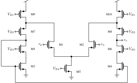
Figure 4: Folded cascode OTA
\[A \approx g_{m1} \left( g_{m8} r_{ds8} (r_{ds10} \parallel r_{ds2}) \, \parallel \, g_{m6} r_{ds6} r_{ds4} \right)\] \[\omega_{ugf} = \frac{g_{m1}}{C_L}\]Output swing: \(V_{DD} - 4 V_{DSAT}\)
At 0.8 V the folded cascode is possible, but on a diet: four $V_{DSAT}$ of about 0.1 V each leaves 0.4 V of output swing, and the bias voltages $V_{B1}$ to $V_{B3}$ must be generated carefully (wide swing mirrors, see CJM) or the diet fails. It is also the last stop: the telescopic cascode, which stacks the input pair under the cascodes, needs the swing and the input common mode to share headroom that is not there at 0.8 V.
The load capacitor is the compensation - no Miller capacitor needed - so for switched capacitor circuits, where the load is a known sampling capacitor, this topology is the default single stage answer.
Inverter based OTAs
Every topology so far spends half its current on transistors that do not amplify. The inverter, Figure 5, does not: the PMOS and NMOS share the same current, both amplify the same input, and the transconductances add.
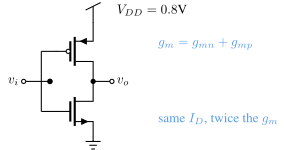
Figure 5: The inverter as a transconductor
The inverter gives $g_{mn} + g_{mp}$ for one branch current - twice the transconductance per microampere of anything above, which at 0.8 V, in weak inversion, is exactly the currency that matters. The catch: an inverter has no tail current source, so its current and its common mode are set by $V_{DD}$ and the process. It rejects nothing - supply noise and corners go straight through.
Nauta showed in 1992 how to make a real OTA out of nothing but inverters, Figure 6 3. Two inverters amplify differentially. On the outputs, a cross coupled pair fights common mode motion and a shorted inverter on each output loads it resistively - together they hold the output common mode without a single tail source or CMFB loop, and the differential gain survives.
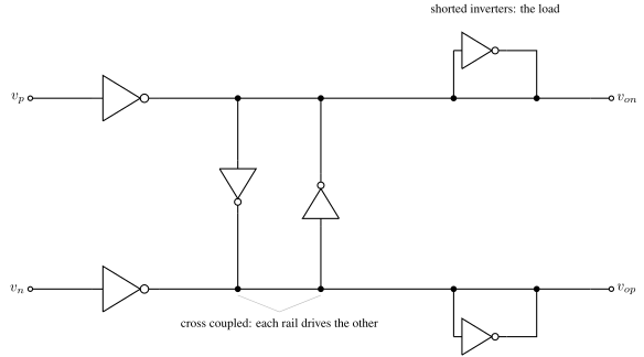
Figure 6: Nauta’s inverter based transconductor
Because every device is part of an inverter, the whole OTA works at any supply where an inverter has gain - which in weak inversion means a few hundred millivolts. Inverter based OTAs run the switched capacitor filters and sigma-delta modulators of most sub-1V papers of the last decade. The supply sensitivity does not disappear, though: it moves into the bias, so the supply of an inverter based OTA is usually a regulated one - see the voltage regulation chapter.
Bulk driven input
One more low voltage trick from the MOSFET chapter: the bulk is a second gate with $g_s \approx 0.2 g_m$, and it works with the source at the rail. Feed the signal into the bulk of a transistor whose $V_{GS}$ is tied fully on, and the input common mode range covers the whole supply - no input pair $V_{GS}$ in the headroom budget at all.
The cost is honest: five times less transconductance for the same current, more input capacitance, and the forward bias diode from bulk to source limits the drive. Bulk driven input stages show up where the input common mode is hostile - rail to rail buffers, sensor interfaces - not where noise or speed matter most.
Bulk as signal input
\[g_{s} \approx (n-1) g_m \approx 0.2 g_m\]Input common mode: rail to rail
Cost: five times less transconductance, and the bulk-source diode must stay off
Fully differential
At 0.8 V, going fully differential is not a luxury, it is where the missing swing went: differential output doubles the signal amplitude for free, cancels even order distortion, and rejects the supply and substrate noise that a single ended output adds to the signal. Figure 7 shows a fully differential current mirror OTA.
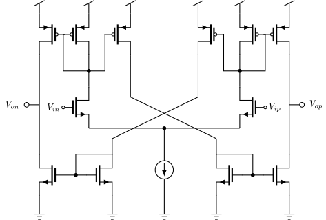
Figure 7: Fully differential current mirror OTA
The price of removing the diode connected definition of the output: the output common mode is no longer defined by the circuit itself. Both outputs can drift towards a rail together, and the differential loop cannot see it. Every fully differential OTA therefore carries a common mode feedback (CMFB) loop.
Common mode feedback
The CMFB loop in Figure 8 senses the average of the two outputs, compares it against a reference - usually mid supply - and trims a bias current in the OTA until the average sits where it should. The loop must be stable on its own, and fast enough to catch common mode disturbances, which in switched capacitor circuits usually means a switched capacitor CMFB sensing network.
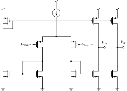
Figure 8: A common mode feedback amplifier
The amplifier of Figure 8 is the continuous time flavor: the output average is sensed, compared against $V_{CREF}$, and the result trims the tail bias. It corrects at every moment, but the sensing network loads the outputs, and at 0.8 V any sensing follower costs headroom.
Sensing the common mode
Figure 9 shows where the two voltages the CMFB amplifier compares come from. Source followers tap $V_{on}$ and $V_{op}$ without loading the outputs resistively, and the resistor network averages the two into the sensed common mode $V_{COUT}$. The reference $V_{CREF}$ is generated the same way - a matching follower off a resistor divider - so the follower’s level shift and its temperature drift cancel in the comparison, and the loop regulates the true output average.
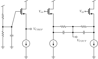
Figure 9: Common mode sense circuit with source followers, and the matching resistor divider generating the reference $V_{CREF}$
Switched capacitor CMFB
In a sampled system the standard answer is the switched capacitor CMFB in Figure 10. The two $C_1$ sense the average of the outputs and level shift it directly onto the tail bias node $v_{cmfb}$ - no amplifier, no headroom, and capacitors are perfectly linear. The switched $C_2$ refresh the level shift towards $V_{cm} - V_B$ on every $\phi_1$, so leakage and startup errors bleed away in a few clock cycles.
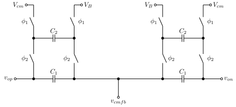
Figure 10: Switched capacitor CMFB
The price is clocked operation: between the phases the common mode is held only by the capacitors, so the loop corrects at the clock rate rather than continuously. In a switched capacitor filter or ADC that clock already exists, which is why nearly every fully differential OTA in a sampled system uses this network.
Bias circuits
Every $V_B$ in this chapter has quietly assumed a bias network. The reference chapter builds the reference current itself; here is how that current becomes the gate voltages the OTAs need, Figure 11.
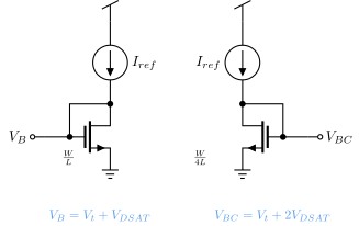
Figure 11: Mirror bias and wide swing cascode bias
The left branch is the workhorse: the reference current into a diode connected device gives $V_B = V_t + V_{DSAT}$, which every tail and mirror gate in this chapter copies. The right branch makes the cascode bias: the same current into a device with a quarter of the $W/L$ needs twice the effective voltage, so its gate sits at $V_t + 2V_{DSAT}$. A cascode gated by $V_{BC}$ then holds its mirror transistor right at the edge of saturation - the wide swing bias that the folded cascode’s 0.4 V of output swing depends on.
Three practical rules come with the schematic. Distribute currents, not voltages: a $V_B$ routed across the chip picks up every IR drop and ground difference on the way, so send a mirrored current and rebuild the voltage locally. Decouple every bias gate to its source rail with a capacitor - the bias node is part of the signal circuit at high frequency. And remember the bias block in the verification below: an OTA that starts before its bias does is an oscillator with ambitions.
From OTA to op amp
An OTA’s output is a current source: high output resistance, happy with a capacitor, helpless into a resistor. The op amp is the same circuit plus an output stage that buys a low output resistance, Figure 12.
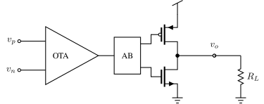
Figure 12: An op amp is an OTA plus an output stage
The class AB block level shifts the two gate drives so both output devices idle at a small quiescent current, yet either can deliver many times that current into the load - power efficiency a class A follower cannot match. At 0.8 V the output pair is drawn as two common source devices, because source followers no longer fit: a follower costs a full $V_{GS}$ of swing, the common source pair costs one $V_{DSAT}$ per rail.
On chip, almost every load is a capacitor or a switched capacitor, so inside the chip you nearly always want the OTA and its high output resistance - the loop gain is free gain. The op amp earns its output stage at the pad ring: reference buffers, regulator error amplifiers driving pass devices, anything that leaves the die.
A complete OTA, sized
To make all of this concrete, Figure 13 shows a fully differential two-stage OTA that will drive most switched capacitor circuits, with every device sized. The notation is “WFLF”: 24F4F means the width is 24 and the length 4 minimum gate lengths, so the same schematic ports between processes by re-reading F. Only one side is drawn - the other half mirrors it.
All the pieces of this chapter appear at once: a cascoded PMOS tail into the input pair, a cascoded current mirror load making the first stage output, a common source second stage with its 500 fF compensation capacitor returned to the cascode source instead of the gate - the cascoded Miller trick that hides the RHP zero - and, on the left, the CMFB amplifier. The outputs are sensed with 60k||20f networks (the capacitor keeps the sense path fast where the resistor divider rolls off), compared against a 100k/100k mid-supply divider, and the correction is injected in parallel with the VBP bias of the first stage load.
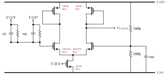
Figure 13: The common mode feedback amplifier. VON and VOP are sensed through 60k||20f networks and compared against a 100k/100k mid-supply reference. Each load PMOS is diode connected on its own - the gates are not tied together - so the gain is the modest, well defined $g_{mn}/g_{mp}$ that a common mode loop wants, and the correction leaves as $V_{CMFB}$
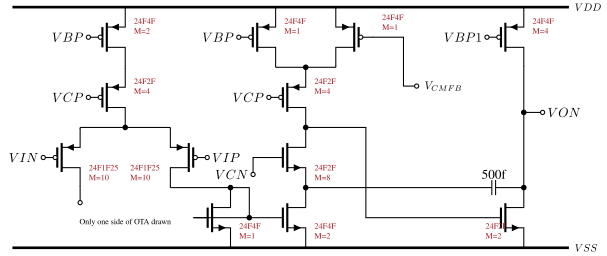
Figure 14: The OTA itself, one side drawn, sized in multiples of the minimum gate length F: a cascoded PMOS tail into the input pair, a cascoded mirror making the first stage output, and a common source second stage with 500 fF of cascode compensation. $V_{CMFB}$ arrives from the amplifier in Figure 13
The bias generator in Figure 15 turns a 10 uA reference into the five gate voltages the OTA asked for. A diode connected NMOS sets the mirror line; one PMOS branch with a diode on top makes VBP; a long channel PMOS diode straight off the supply drops enough V_GS to make the cascode bias VCP, and its NMOS twin makes VCN; a stack of two NMOS diodes makes VBN for the tails; and a separate PMOS diode makes VBP1 so the second stage can be biased independently of the first.
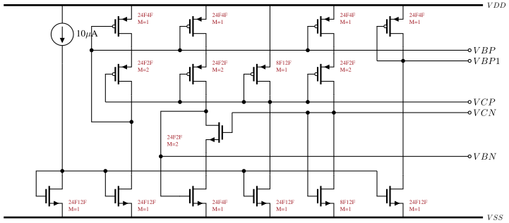
Figure 15: The bias generator. The 10 uA reference is mirrored once in an ordinary current mirror - the line along the bottom - and everything above it is wide swing cascode: the narrow 8F12F devices set VCP and VCN, and in each master the mirror device’s gate hangs on the far end of its own stack
Dynamic amplifiers
The newest branch of the family tree is also, on inspection, one of the oldest: Hosticka showed dynamic CMOS amplifiers already in 1980 4, and scaling has made the idea mainstream. A dynamic amplifier throws away the bias current entirely: it integrates its input onto a capacitor for a clocked instant and then stops. The “gain” is $g_m T / C$, the power is $C V^2 f$, and between samples the amplifier burns nothing. Ring amplifiers 5 do the same with an inverter chain that slams the output and then dead-bands itself into a precision settle.
They only work in sampled systems - a SAR or pipeline ADC stage, a discrete time filter - but there they have taken over: an amplifier that only exists while it is needed is the logical endpoint of the headroom and power budget this chapter started with.
Dynamic gain
\[A \approx \frac{g_m T}{C}\]Power
\[P \propto C V_{DD}^2 f_s\]Only in sampled systems, and everywhere in modern ADCs
Choosing
| Topology | Gain | Swing | Best at |
|---|---|---|---|
| Five transistor | \(g_m r_{ds}\) | good | buffers, bias loops |
| Current mirror | \(K g_m r_{ds}\) | good | drive, SC circuits |
| Two stage Miller | \((g_m r_{ds})^2\) | best | gain + swing |
| Folded cascode | \(g_m (g_m r_{ds}^2)\) | poor | SC settling |
| Inverter based | \(g_m r_{ds}\) | good | sub-1V, low power |
| Dynamic | \(g_m T/C\) | - | ADCs |
Read the table bottom up: at 0.8 V the pressure is towards the bottom rows. Start with the five transistor OTA, and move only when a measured, simulated shortfall - gain, swing, drive, power - pushes you to a specific neighbor.
Verifying the OTA
Designing the OTA is the smaller half of the work. Before it goes into a system, a standard battery of analyses must say yes - and each row below has a reason to exist, usually a chip that failed without it.
| Analysis | Testbench | Look for |
|---|---|---|
| Operating point | closed loop, DC | every device saturated, all corners |
| Loop gain | stb / broken loop | DC gain, UGF, phase margin > 60 deg |
| CMFB loop gain | stb on the CM loop | stable on its own, faster than the disturbance |
| Noise | AC noise, closed loop | input referred, thermal and flicker |
| Offset | Monte Carlo mismatch | sigma of input referred offset |
| Swing | sweep output, plot gain | where the gain collapses |
| Slew and settling | large signal step | settles to accuracy in the time budget |
| PSRR / CMRR | AC from supply / CM | worst case versus frequency |
| Start-up | transient from zero | bias and CMFB wake up, always |
| Power | DC, all corners | the budget holds where it is slowest |
A few of the rows deserve their own sentence.
The operating point check is first because it is cheap and catches most disasters: a single transistor pushed into triode at the slow-slow, low supply, hot corner explains many a “the gain is 20 dB too low in the lab” story. Check it across corners, supplies and temperature before trusting any small signal number.
The loop gain must be measured with the loading in place - the real feedback network, the real sampling capacitors - because the phase margin depends on the load more than on the OTA. For a fully differential OTA there are two loops, and the CMFB loop must be analyzed separately: it has its own crossover and its own phase margin, and an unstable CMFB loop looks exactly like an oscillating OTA.
Offset and noise are budget items, not pass/fail: Monte Carlo gives the offset sigma that the system - a comparator threshold, an ADC code - must absorb, and the input referred noise integrated over the signal band must sit under the quantization or thermal floor it feeds.
Slew and settling only exist in a large signal transient. The small signal bandwidth promises nothing about a full scale step: the input pair steers all its tail current, the OTA slews at $I/C$, and only the last stretch is exponential. In a switched capacitor circuit the settling budget is half a clock period, and it is the transient - with mismatch, with corners - that says whether the budget holds.
And start-up: simulate the whole thing from zero supply, every time. Bias loops and CMFB loops both have a stable state called “off”, and finding it in silicon is the most expensive way to learn this rule.
Summary
The one-page version of this chapter:
- At 0.8 V: never stack two gate-source voltages, and count every saturation voltage
- Five transistor OTA first; upgrade only for a reason
- Need drive: current mirror OTA. Need gain: two stage. Need one-stage gain: folded cascode
- Miller compensation splits the poles; the unity gain frequency is gm over Cc; mind the RHP zero
- Inverters amplify: both transconductances for one branch current, and Nauta’s OTA needs no tail
- Fully differential doubles swing but must pay the CMFB tax
- In sampled systems, dynamic amplifiers win the power argument
Would you like to know more?
The paper that named the transconductance amplifier and argued it would obsolete the op amp 1
OTA-based filter design, the reason the OTA became a building block rather than a curiosity 2
Nauta’s inverter transconductor, drawn in this chapter, with the analysis of why its common mode holds 3
Dynamic CMOS amplifiers, twenty years before the idea became mainstream 4
Ring amplifiers, where the dynamic branch of the family went 5
-
C. F. Wheatley and H. A. Wittlinger, OTA Obsoletes OP. AMP. 1969 https://class.ece.iastate.edu/ee435/miscHandouts/OTA%20Wheatley%20and%20Wittlinger%20Dec%2069.pdf ↩ ↩2
-
R. L. Geiger and E. Sánchez-Sinencio, Active Filter Design Using Operational Transconductance Amplifiers: A Tutorial 1985 https://doi.org/10.1109/MCD.1985.6311946 ↩ ↩2
-
Bram Nauta, A CMOS transconductance-C filter technique for very high frequencies 1992 https://doi.org/10.1109/4.127337 ↩ ↩2
-
B. J. Hosticka, Dynamic CMOS amplifiers 1980 https://doi.org/10.1109/JSSC.1980.1051488 ↩ ↩2
-
B. Hershberg and S. Weaver and K. Sobue and S. Takeuchi and K. Hamashita and U.-K. Moon, Ring Amplifiers for Switched Capacitor Circuits 2012 https://doi.org/10.1109/JSSC.2012.2217865 ↩ ↩2