Table of contents
Keywords: SC DAC, SC FUND, DT, Alias, Subsample, Z Domain, FIR, IIR, SC MDAC, SC INT, Switch, Non-Overlap, VBE SC, Nyquist
Active-RC
A general purpose Active-RC bi-quadratic (two-quadratic equations) filter is shown below
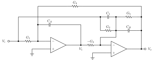
Figure 1: General purpose Active-RC biquad
If you want to spend a bit of time, then try and calculate the transfer function below.
\[H(s) = \frac{\left[ \frac{C_1}{C_B}s^2 + \frac{G_2}{C_B}s + (\frac{G_1G_3}{C_A C_B})\right]}{\left[ s^2 + \frac{G_5}{C_B}s + \frac{G_3 G_4}{C_A C_B}\right]}\]Active resistor capacitor filters are made with OTAs (high output impedance) or OPAMP (low output impedance). Active amplifiers will consume current, and in Active-RC the amplifiers are always on, so there is no opportunity to reduce the current consumption by duty-cycling (turning on and off).
Both resistors and capacitors vary on an integrated circuit, and the 3-sigma variation can easily be 20 %.
The pole or zero frequency of an Active-RC filter is proportional to the inverse of the product between R and C
\[\omega_{p\vert z} \propto \frac{G}{C} = \frac{1}{RC}\]As a result, the total variation of the pole or zero frequency can have a 3-sigma value of
\[\sigma_{RC} = \sqrt{ \sigma_R^2 + \sigma_C^2 } = \sqrt{0.2^2 + 0.2^2} = 0.28 = 28 \text{ \%}\]On an IC we sometimes need to calibrate the R or C in production to get an accurate RC time constant.
We cannot physically change an IC, every single one of the 100 million copies of an IC is from the same Mask set. That’s why ICs are cheap. To make the Mask set is incredibly expensive (think 5 million dollars), but a copy made from the Mask set can cost one dollar or less. To calibrate we need additional circuits.
Imagine we need a resistor of 1 kOhm. We could create that by parallel connection of larger resistors, or series connection of smaller resistors. Since we know the maximum variation is 0.02, then we need to be able to calibrate away +- 20 Ohms. We could have a 980 Ohm resistor, and then add ten 4 Ohm resistors in series that we can short with a transistor switch.
But is a resolution of 4 Ohms accurate enough? What if we need a precision of 0.1%? Then we would need to tune the resistor within +-1 Ohm, so we might need 80 0.5 Ohm resistors.
But how large is the on-resistance of the transistor switch? Would that also affect our precision?
But is the calibration step linear with addition of the transistors? If we have a non-linear calibration step, then we cannot use gradient descent calibration algorithms, nor can we use binary search.
Analog designers need to deal with an almost infinite series of “But”.
The experienced designer will know when to stop, when is the “But what if” not a problem anymore.
The most common error in analog integrated circuit design is a “I did not imagine that my circuit could fail in this manner” type of problem. Or, not following the line of “But”’s far enough.
But if we follow all the “But”’s we will never tapeout!
Active-RC filters are great for linearity, but if we need accurate time constant, there are better alternatives.
Gm-C
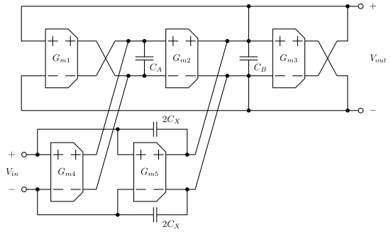
Figure 2: General purpose Gm-C biquad
\[H(s) = \frac{\left[ s^2\frac{C_X}{C_X + C_B} + s\frac{G_{m5}}{C_X + C_B} + \frac{G_{m2}G_{m4}}{C_A(C_X + C_B)}\right]} {\left[s^2 + s\frac{G_{m3}}{C_X + C_B} + \frac{G_{m1}G_{m2}}{C_A(C_X + C_B)} \right]}\]The pole and zero frequency of a Gm-C filter is
\[\omega_{p\vert z} \propto \frac{G_m}{C}\]The transconductance accuracy depends on the circuit, and the bias circuit, so we can’t give a general, applies for all circuits, sigma number. Capacitors do have 3-sigma 20 % variation, usually.
Same as Active-RC, Gm-C need calibration to get accurate pole or zero frequency.
Switched capacitor
The first time you encounter Switched Capacitor (SC) circuits, they do require some brain training. So let’s start simple.
Consider the circuit below. Assume that the two transistors are ideal (no-charge injection, no resistance).
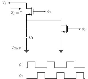
Figure 3: Switched capacitor with two transistor switches and the non-overlapping clock phases $\phi_1$ and $\phi_2$
For SC circuits, we need to consider the charge on the capacitors, and how they change with time.
The charge on the capacitor at the end 1 of phase 2 is
\[Q_{\phi2\$} = C_1 V_{GND} = 0\]while at the end of phase 1
\[Q_{\phi1\$} = C_1 V_{I}\]The impedance, from Ohm’s law is
\[Z_{I} = (V_{I} - V_{GND})/I_{I}\]And from SI units units we can see current is charge per unit time. Once per clock period the capacitor is charged and then discharged, so what flows in from the input is the difference between the charge held at the end of each phase, delivered $f_\phi$ times a second:
\[I_{I} = \frac{\Delta Q}{\Delta t} = \left(Q_{\phi1\$} - Q_{\phi2\$}\right) f_{\phi}\]Charge cannot disappear, charge is conserved. As such, the charge going out from the input must be equal to the difference of charge at the end of phase 1 and phase 2.
\[Z_{I} = \frac{V_{I} - V_{GND}}{\left(Q_{\phi1\$} - Q_{\phi2\$}\right) f_{\phi}}\]Inserting for the charges, we can see that the impedance is
\[Z_{I} = \frac{V_{I}}{\left(C_1 V_{I} - 0 \right) f_{\phi}} = \frac{1}{C_1 f_\phi}\]A common confusion with SC circuits is to confuse the impedance of a capacitor $Z = 1/sC$ with the impedance of a SC circuit $Z = 1/fC$. The impedance of a capacitor is complex (varies with frequency and time), while the SC circuit impedance is real (a resistance).
The main difference between the two is that the impedance of a capacitor is continuous in time, while the SC circuit is a discrete time circuit, and has a discrete time impedance.
The circuit below is drawn slightly differently, but the same equation applies.
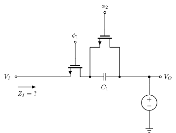
Figure 4: The same switched capacitor rotated, now between the input and an output voltage source
If we compute the impedance.
\[Z_{I} = \frac{V_{I} - V_{O}}{\left(Q_{\phi1\$} - Q_{\phi2\$}\right) f_{\phi}}\] \[Q_{\phi1\$} = C_1 (V_I - V_O)\] \[Q_{\phi2\$} = 0\] \[Z_{I} = \frac{V_{I} - V_{O}}{C_1 \left(V_I - V_O\right) f_{\phi}} = \frac{1}{C_1 f_\phi}\]Which should not be surprising, as all I’ve done is to rotate the circuit and call $V_{GND} = V_0$.
Let’s try the circuit below.
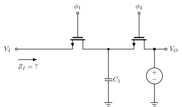
Figure 5: Switched capacitor with series switches, charging $C_1$ to $V_I$ in $\phi_1$ and $V_O$ in $\phi_2$
\[Z_{I} = \frac{ V_{I} - V_{O} }{ \left(Q_{\phi1\$} - Q_{\phi2\$}\right) f_{\phi}}\] \[Q_{\phi1\$} = C_1 V_I\] \[Q_{\phi2\$} = C_1 V_O\]Inserted into the impedance we get the same result.
\[Z_{I} = \frac{V_{I} - V_{O}}{\left(C_1 V_I - C_1 V_O\right) f_{\phi}} = \frac{1}{C_1 f_\phi}\]The first time I saw the circuit above it was not obvious to me that the impedance still was $Z = 1/Cf$. It’s one of the cases where mathematics is a useful tool. I could follow a set of rules (charge conservation), and as long as I did the mathematics right, then from the equations, I could see how it worked.
An example SC circuit
An example use of an SC circuit is
A pipelined 5-Msample/s 9-bit analog-to-digital converter 2
Shown in the figure below. You should think of the switched capacitor circuit as similar to an amplifier with constant gain. We can use two resistors and an opamp to create a gain. Imagine we create a circuit without the switches, and with a resistor of $R$ from input to virtual ground, and $4R$ in the feedback. Our Active-R would have a gain of $A = 4$.
The switches disconnect the OTA and capacitors for half the time, but for the other half, at least for the latter parts of $\phi_2$ the gain is four.
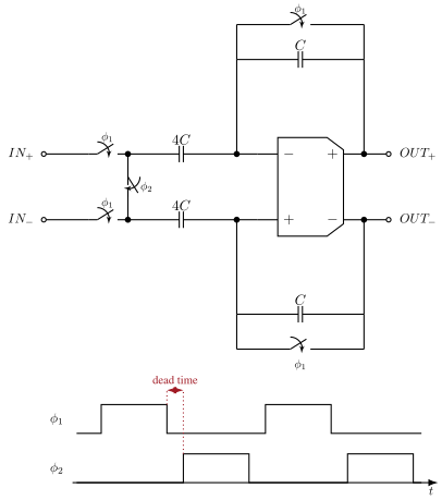
Figure 6: A fully differential switched-capacitor sample-and-hold with a gain of four, and the two-phase clock that runs it. On $\phi_2$ the two input plates are shorted to each other rather than to ground, which discharges the common mode while leaving the differential charge alone. Inspired by Fig. 6 of Lewis and Gray 2
Follow the charge and the gain falls out. During $\phi_1$ the input is sampled onto $4C$ while the reset switch shorts $C$, so the feedback capacitor starts empty. During $\phi_2$ the two left plates are shorted to each other, so they settle to whatever common voltage the pair demands, and the differential charge that was on them, $4C V_{in}$, has nowhere to go except onto $C$ — the OTA’s inputs are high impedance and its own feedback holds them together. Charge conservation then gives $C V_{out} = 4C V_{in}$, so the gain is 4, and it is 4 because one capacitor is four times another rather than because any transistor did something particular.
Shorting the plates to each other rather than to ground is not a detail. Ground is a different node at each end of the chip, and any difference between the two would be sampled straight into the signal; shorting the pair to itself discharges the common mode without ever consulting ground, which is where the common mode rejection of this circuit comes from.
The real circuit in the paper carries a common-mode feedback network and a dummy switch beside every real one, both left out here. They matter enormously when you build it and not at all when you are working out what it does.
The output is only correct for a finite, but periodic, time interval. The circuit is discrete time. As long as all circuits afterwards also have a discrete-time input, then it’s fine. An ADC can sample the output from the amplifier at the right time, and never notice that the output is shorted to a DC voltage in $\phi_1$
We charge the capacitor $4C$ to the differential input voltage in $\phi_1$
\[Q_1 = 4 C V_{in}\]Then we turn off $\phi_1$, which opens all switches. The charge on $4C$ will still be $Q_1$ (except for higher order effects like charge injection from switches).
After a short time (non-overlap), we turn on $\phi_2$, closing some of the switches. The OTA will start to force its two inputs to be the same voltage, and we short the left side of $4C$. After some time we would have the same voltage on the left side of $4C$ for the two capacitors, and another voltage on the right side of the $4C$ capacitors. The two capacitors must now have the same charge, so the difference in charge, or differential charge must be zero.
Physics tell us that charge is conserved, so our differential charge $Q_1$ cannot vanish into thin air. The difference in electrons that made $Q_1$ must be somewhere in our circuit.
Assume the designer of the circuit has done a proper job, then the $Q_1$ charge will be found on the feedback capacitors.
We now have a $Q_1$ charge on smaller capacitors, so the differential output voltage must be
\[Q_1 = 4 C V_{in} = Q_2 = C V_{out}\]The gain is
\[A = \frac{V_{out}}{V_{in}} = 4\]Why would we go to all this trouble to get a gain of 4?
In general, we can sum up with the following equation.
\[\omega_{p\vert z} \propto f_{clk}\frac{C_1}{C_2}\]We can use these “switched capacitor resistors” to get pole or zero frequency or gain proportional to the relative size of capacitors, which is a fantastic feature. Assume we make two identical capacitors in our layout. We won’t know the absolute size of the capacitors on the integrated circuit, whether the $C_1$ is 100 fF or 80 fF, but we can be certain that if $C_1 = 80$ fF, then $C_2 = 80$ fF to a precision of around 0.1 %.
With switched capacitor amplifiers we can set an accurate gain, and we can set an accurate pole and zero frequency (as long as we have an accurate clock and a high DC gain OTA).
The switched capacitor circuits do have a drawback. They are discrete time circuits. As such, we must treat them with caution, and they will always need some analog filter before to avoid a phenomena we call aliasing.
Discrete-Time Signals
An random, Gaussian, continuous time, continuous value, signal has infinite information. The frequency can be anywhere from zero to infinity, the value have infinite levels, and the time division is infinitely small. We cannot store such a signal. We have to quantize.
If we quantize time to $T = 1\text{ ns}$, such that we only record the value of the signal every 1 ns, what happens to all the other information? The stuff that changes at 0.5 ns or 0.1 ns, or 1 ns.
We can always guess, but it helps to know, as in absolutely know, what happens. That’s where mathematics come in. With mathematics we can prove things, and know we’re correct.
The mathematics
Define \(x_c (t)\) as a continuous time, continuous value signal
Define \(\ell(t) = \begin{cases} 1 & \text{if } t \geq 0 \\ 0 & \text{if } t < 0 \end{cases}\)
Define \(x_{sn}(t) = \frac{x_c(nT)}{\tau}[\ell(t-nT) - \ell(t - nT - \tau)]\)
where $x_{sn}(t)$ is a function of the continuous time signal at the time interval $nT$.
Define \(x_s(t) = \sum_{n=-\infty}^{\infty}{x_{sn}(t)}\)
where $x_s(t)$ is the sampled, continuous time, signal.
Think of a sampled version of an analog signal as an infinite sum of pulse trains where the area under the pulse train is equal to the analog signal.
Why do this?
With a exact definition of a sampled signal in the time-domain it’s sometimes possible to find the Laplace transform, and see how the frequency spectrum looks.
If \(x_s(t) = \sum_{n=-\infty}^{\infty}{x_{sn}(t)}\)
Then \(X_{sn}(s) = \frac{1}{\tau}\frac{1 - e^{-s\tau}}{s} x_c(nT)e^{-snT}\)
And \(X_s(s) = \frac{1}{\tau}\frac{1 - e^{-s\tau}}{s} \sum_{n=-\infty}^{\infty}x_c(nT)e^{-snT}\)
Thus \(\lim_{\tau \to 0} \rightarrow X_s(s) = \sum_{n=-\infty}^{\infty}x_c(nT)e^{-snT}\)
The spectrum of a sampled signal is an infinite sum of frequency shifted spectra
or equivalently
When you sample a signal, then there will be copies of the input spectrum at every \(nf_s\)
However, if you do an FFT of a sampled signal, then all those infinite spectra will fold down between \(0 \to f_{s1}/2\) or \(- f_{s1}/2 \to f_{s1}/2\) for a complex FFT
Python discrete time example
If your signal processing skills are a bit thin, now might be a good time to read up on FFT, Laplace transform and But what is the Fourier Transform?
In python we can create a demo and see what happens when we “sample” a “continuous time” signal. Hopefully it’s obvious that it’s impossible to emulate a “continuous time” signal on a digital computer. After all, it’s digital (ones and zeros), and it has a clock!
We can, however, emulate to any precision we want.
The code below has four main sections. First is the time vector. I use Numpy, which has a bunch of useful features for creating ranges, and arrays.
Secondly, I create continuous time signal. The time vector can be used in numpy functions, like np.sin(), and I combine three sinusoid plus some noise. The sampling vector is a repeating pattern of 11000000, so our sample rate is 1/8’th of the input sample rate. FFT’s can be unwieldy beasts. I like to use coherent sampling, however, here the tone is deliberately placed halfway between two FFT bins, so the record is not coherent.
The alternative to coherent sampling is to apply a window function before the FFT, that’s the reason for the Hanning window below.
There is an interactive version of this example where the tone frequency, the sampling pattern and the window are sliders. Turning the Hanning window off, and then turning coherent sampling on, is worth thirty seconds of your time.
#- Create a time vector
N = 2**13
t = np.arange(N)

#- Create the "continuous time" signal with multiple
#- "sinusoidal signals and some noise
#- f1 is deliberately halfway between FFT bins, so the
#- record is not coherent and the window has a job to do
f1 = 233.5/N
fd = 1/N*119
x_s = np.sin(2*np.pi*f1*t) + 1/1024*np.random.randn(N) + \
    0.5*np.sin(2*np.pi*(f1-fd)*t) + 0.5*np.sin(2*np.pi*(f1+fd)*t)

#- Create the sampling vector, and the sampled signal
t_s_unit = [1,1,0,0,0,0,0,0]
t_s = np.tile(t_s_unit,int(N/len(t_s_unit)))
x_sn = x_s*t_s

#- Convert to frequency domain with a hanning window to avoid FFT bin
#- energy spread
Hann = True
if(Hann):
    w = np.hanning(N+1)
else:
    w = np.ones(N+1)
X_s = np.fft.fftshift(np.fft.fft(np.multiply(w[0:N],x_s)))
X_sn = np.fft.fftshift(np.fft.fft(np.multiply(w[0:N],x_sn)))
Try to play with the code, and see if you can understand what it does.
Below are the plots. On the left side is the “continuous value, continuous time” emulation, on the right side “discrete time, continuous value”.
The top plots are the time domain, while the bottom plots is frequency domain.
The FFT is complex, so that’s why there are six sinusoids bottom left. The frequency axis is normalized to the sample rate, so it runs from $-f_s/2$ to $+f_s/2$ with 0 Hz in the middle.
The spectral copies can be seen bottom right. How many spectral copies, and the distance between them will depend on the sample rate (length of t_s_unit). Try to play around with the code and see what happens.
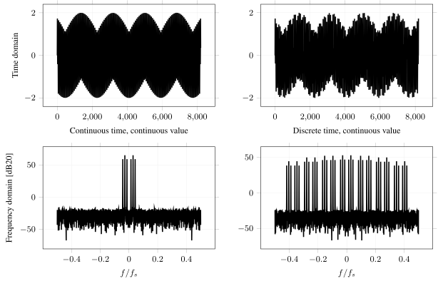
Figure 7: Time domain and spectrum of the emulated continuous time signal (left) and the sampled signal with its spectral copies (right)
Aliasing, bandwidth and sample rate theory
I want you to internalize that the spectral copies are real. They are not some “mathematical construct” that we don’t have to deal with.
They are what happens when we sample a signal into discrete time. Imagine a signal with a band of interest as shown below in Green. We sample at $f_s$. The pink and red unwanted signals do not disappear after sampling, even though they are above the Nyquist frequency ($f_s/2$). They fold around $f_s/2$, and may appear in-band. That’s why it’s important to band limit analog signals before they are sampled.
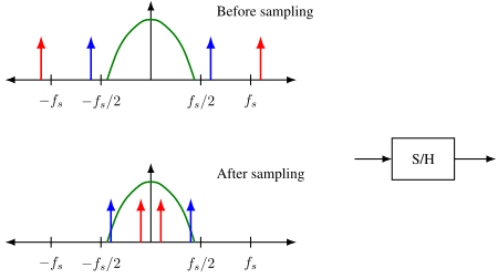
Figure 8: Spectrum before and after sampling: unwanted signals above $f_s/2$ fold into the wanted band
With an anti-alias filter (yellow) we ensure that the unwanted components are low enough before sampling. As a result, our wanted signal (green) is undisturbed.
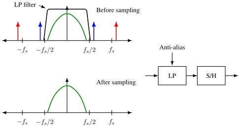
Figure 9: An anti-alias low-pass filter attenuates the unwanted components before sampling
Assume that we’re interested in the red signal. We could still use a sample rate of $f_s$. If we bandpass-filtered all but the red signal the red signal would fold on sampling, as shown in the figure below.
Remember that the Nyquist-Shannon states that a sufficient no-loss condition is to sample signals with a sample rate of twice the bandwidth of the signal.
Nyquist-Shannon has been extended for sparse signals, compressed sensing, and non-uniform sampling to demonstrate that it’s sufficient for the average sample rate to be twice the bandwidth. One 2009 paper Blind Multiband Signal Reconstruction: Compressed Sensing for Analog Signal 3 is a good place to start to delve into the latest on signal reconstruction.
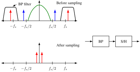
Figure 10: Sub-sampling: a band-pass filtered signal above $f_s/2$ folds down to low frequency on sampling
Z-transform
Someone got the idea that writing
\[X_s(s) = \sum_{n=-\infty}^{\infty}x_c(nT)e^{-snT}\]was cumbersome, and wanted to find something better.
\[X_s(z) = \sum_{n=-\infty}^{\infty}x_c[n]z^{-n}\]For discrete time signal processing we use Z-transform
If you’re unfamiliar with the Z-transform, read the book or search https://en.wikipedia.org/wiki/Z-transform
The nice thing with the Z-transform is that the exponent of the z tell’s you how much delayed the sample $x_c[n]$ is. A block that delays a signal by 1 sample could be described as $x_c[n] z^{-1}$, and an accumulator
\[y[n] = y[n-1] + x[n]\]in the Z domain would be
\[Y(z) = z^{-1}Y(z) + X(z)\]With a Z-domain transfer function of
\[\frac{Y(z)}{X(z)} = \frac{1}{1 - z^{-1}}\]Pole-Zero plots
If you’re not comfortable with pole/zero plots, have a look at
What does the Laplace Transform really tell us
Think about the pole/zero plot as a surface your looking down onto. At $a = 0$ we have the steady state fourier transform. The “x” shows the complex frequency where the fourier transform goes to infinity.
Any real circuit will have complex conjugate, or real, poles/zeros. A combination of two real circuits where one path is shifted 90 degrees in phase can have non-conjugate complex poles/zeros.
If the “x” is $a<0$, then any perturbation will eventually die out. If the “x” is on the $a=0$ line, then we have a oscillator that will ring forever. If the “x” is $a>0$ then the oscillation amplitude will grow without bounds, although, only in Matlab. In any physical circuit an oscillation cannot grow without bounds forever.
Growing without bounds is the same as “being unstable”.
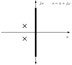
Figure 11: A complex conjugate pole pair in the s-plane
Z-domain
Spectra repeat every \(2\pi\)
As such, it does not make sense to talk about a plane with a $a$ and a $j\omega$. Rather we use the complex number $z = a + jb$.
As long as the poles (“x”) are within the unit circle, oscillations will die out. If the poles are on the unit-circle, then we have an oscillator. Outside the unit circle the oscillation will grow without bounds, or in other words, be unstable.
We can translate between Laplace-domain and Z-domain with the Bi-linear transform
\[s = \frac{2}{T}\frac{z -1}{z + 1}\]Warning: First-order approximation https://en.wikipedia.org/wiki/Bilinear_transform
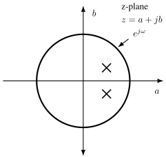
Figure 12: The z-plane with the unit circle and a complex conjugate pole pair
First order filter
Assume a first order filter given by the discrete time equation.
\[y[n+1] = bx[n] + ay[n] \Rightarrow Y z = b X + a Y\]The “n” index and the “z” exponent can be chosen freely, which sometimes can help the algebra.
\[y[n] = b x[n-1] + ay[n-1] \Rightarrow Y = b X z^{-1} + a Y z^{-1}\]The transfer function can be computed as
\[H(z) = \frac{b}{z-a}\]From the discrete time equation we can see that the impulse will never die out. We’re adding the previous output to the current input. That means the circuit has infinite memory. Accordingly, filters of this type are known as. Infinite-impulse response (IIR)
\[h[n] = \begin{cases} k & \text{if } n < 1 \\ a^{n-1}b + a^n k & \text{if } n \geq 1 \end{cases}\]Head’s up: Fig 13.12 in AIC is wrong
Here $k$ is the initial state $y[0]$. From the impulse response it can be seen that the pole of $H(z) = b/(z-a)$ sits at $z = a$, and $b$ only scales the output, so everything depends on $\vert a\vert$.
Three cases, matching the z-plane picture above. If $\vert a\vert < 1$ the response decays and the filter is stable. If $\vert a\vert > 1$ it grows without bound and the filter is unstable. Exactly on the unit circle, $\vert a\vert = 1$, it neither decays nor grows: the impulse rings for ever at constant amplitude, which is an oscillator. That last case is called marginally stable, and in a real circuit it does not exist — component tolerance will push the pole to one side or the other, and only one of those sides is survivable.
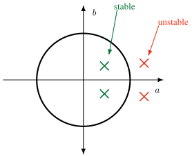
Figure 13: Poles inside the unit circle are stable, poles outside are unstable
Second order filter
A single real pole can only do so much. If we feed back two delayed outputs
\[y[n] = b x[n-1] + 2a\, y[n-1] - (a^2 + b^2)\, y[n-2]\] \[H(z) = \frac{b z}{z^2 - 2a z + (a^2+b^2)}\]then the denominator factors as $(z - z_p)(z - z_p^*)$ with a complex conjugate pole pair at
\[z_p = a + jb\]which is exactly the complex frequency from the Z-domain plot earlier. As long as $\vert a + jb\vert < 1$ the poles are inside the unit circle and the filter is stable. Complex poles also mean the magnitude response peaks near the pole angle — the filter resonates.
The second order filter can be implemented in python, and it’s really not hard. See below. The $x_sn$ vector is from the previous python example.
There are smarter, and faster ways to do IIR filters (and FIR) in python, see scipy.signal.iirfilter
From the plot below we can see the sampled time domain and spectra on the left, and the filtered time domain and spectra on the right. The two spectra share the same y-axis, so the attenuation can be read directly. The poles sit at $0.85 \pm j0.25$ ($\vert z\vert = 0.89$, pole angle $\approx 0.046\,f_s$): the image near the pole angle is picked out and even amplified a little by the resonance, while the spectral copies further out drop with 40 dB/decade.
The interactive version of this example adds the pole position as a slider, and draws the z-plane next to the spectrum, so you can watch the pole move inside the unit circle and the corner frequency follow it.
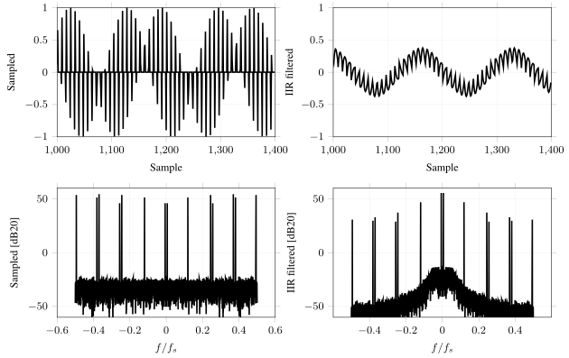
Figure 14: Time domain and spectrum of the sampled signal (left) and the second order IIR filtered output (right)
#- Second-order IIR filter with a complex conjugate
#- pole pair at z = a +/- jb. Stable if |a + jb| < 1.
b = 0.25
a = 0.85
z = a + 1j*b
z_abs = np.abs(z)
print("|z| = " + str(z_abs))
y = np.zeros(N)
for i in range(2,N):
    y[i] = b*x_sn[i-1] + 2*a*y[i-1] - (a*a + b*b)*y[i-2]
The IIR filter we implemented above is a resonant low-pass filter: it picks out the image near its pole angle and rejects the copied spectra further out, as expected.
Finite-impulse response(FIR)
FIR filters are unconditionally stable, since the impulse response will always die out. FIR filters are a linear sum of delayed inputs.
In my humble opinion, there is nothing wrong with an IIR. Yes, they could become unstable, however, they can be designed safely. I’m not sure there is a theological feud on IIR vs FIR, I suspect there could be. Talk to someone that knows digital filters better than me.
But be wary of rules like “IIR are always better than FIR” or vice versa. Especially if statements are written in books. Remember that the book was probably written a decade ago, and based on papers two decades old, which were based on three decades old state of the art. Our abilities to use computers for design has improved a bit the last three decades.
The simplest useful FIR is a moving average. Take the current sample and the two before it, weight each by a third, and add them. There is no feedback path anywhere in it, so a disturbance can only live for as many samples as there are taps, and then it is gone. That is the whole of the stability argument.
\[H(z) = \frac{1}{3}\sum_{i=0}^2 z^{-i} = \frac{1}{3}\left(1 + z^{-1} + z^{-2}\right)\]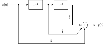
Figure 15: FIR filter summing the input and two delayed samples, each weighted by 1/3
Switched-Capacitor
Below is an example of a switched-capacitor circuit during phase 1. Think of the two phases as two different configurations of a circuit, each with a specific purpose.
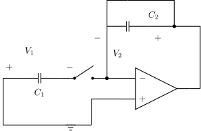
Figure 16: SC circuit during phase 1: $V_1$ is stored on $C_1$ while $C_2$ is shorted
This is the SC circuit during the sampling phase. Imagine that we somehow have stored some voltage $V_1$ on capacitor $C_1$ (the switches for that sampling or storing are not shown). The charge on $C_1$ is
\[Q_{1\phi_1\$} = C_1 V_1\]The $C_2$ capacitor is shorted, as such, $V_2 = 0$, which must mean that the charge on $C_2$ given by
\[Q_{2\phi_1\$} = 0\]The voltage at the negative input of the OTA must be 0 V, as the positive input is 0 V, and we assume the circuit has settled all transients.
Imagine we (very carefully) open the circuit around $C_2$ and close the circuit from the negative side of $C_1$ to the OTA negative input, as shown below.
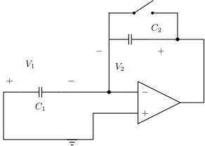
Figure 17: SC circuit during phase 2: the OTA transfers the charge from $C_1$ to $C_2$
It’s the OTA that ensures that the negative input is the same as the positive input, but the OTA cannot be infinitely fast. At the same time, the voltage across $C_1$ cannot change instantaneously. Neither can the voltage across $C_2$. As such, the voltage at the negative input must immediately go to $-V_1$ (ignoring any parasitic capacitance at the negative input).
The OTA does not like its inputs to be different, so it will start to charge $C_2$ to increase the voltage at the negative input to the OTA. When the negative input reaches 0 V the OTA is happy again. At that point the charge on $C_1$ is
\[Q_{1\phi_2\$} = 0\]A key point is that even though the voltages have now changed, there is zero volts across $C_1$, and thus there cannot be any charge on $C_1$. The charge that was there cannot have disappeared. The negative input of the OTA is a high impedance node, and cannot supply charge. The charge must have gone somewhere, but where?
In process of changing the voltage at the negative input of the OTA we’ve changed the voltage across $C_2$. The voltage change must exactly match the charge that was across $C_1$, as such
\[Q_{2\phi_2\$} = Q_{1\phi_1\$} = C_1 V_1 = C_2 V_2\]thus
\[\frac{V_2}{V_1} = \frac{C_1}{C_2}\]Switched capacitor gain circuit
Redrawing the previous circuit, and adding a few more switches we can create a switched capacitor gain circuit.
There is now a switch to sample the input voltage across $C_1$ during phase 1 and reset $C_2$. During phase 2 we configure the circuit to leverage the OTA to do the charge transfer from $C_1$ to $C_2$.
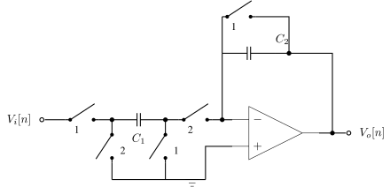
Figure 18: Switched capacitor gain circuit sampling $V_i$ on $C_1$ in phase 1 and transferring the charge to $C_2$ in phase 2
The discrete time output from the circuit will be as shown below. It’s only at the end of the second phase that the output signal is valid. As a result, it’s common to use the sampling phase of the next circuit close to the end of phase 2.
For charge to be conserved the clocks for the switch phases must never be high at the same time.
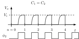
Figure 19: Discrete time output of the gain circuit, only valid towards the end of phase 2
The discrete time, Z-domain and transfer function is shown below. The transfer function tells us that the circuit is equivalent to a gain, and a delay of one clock cycle. The cool thing about switch capacitor circuits is that the precision of the gain is set by the relative size between two capacitors. In most technologies that relative sizing can be better than 0.1 %.
Gain circuits like the one above find use in most Pipelined ADCs, and are common, with some modifications, in Sigma-Delta ADCs.
\[V_o[n+1] = \frac{C_1}{C_2}V_i[n]\] \[V_o z = \frac{C_1}{C_2} V_i\] \[\frac{V_o}{V_i} = H(z) = \frac{C_1}{C_2}z^{-1}\]Switched capacitor integrator
Removing one switch we can change the function of the switched capacitor gain circuit. If we don’t reset $C_2$ then we accumulate the input charge every cycle.
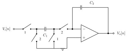
Figure 20: Switched capacitor integrator: without the reset switch the charge accumulates on $C_2$
The output now will grow without bounds, so integrators are most often used in filter circuits, or sigma-delta ADCs where there is feedback to control the voltage swing at the output of the OTA.
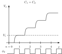
Figure 21: Integrator output growing every clock cycle as the input charge is accumulated
Make sure you read and understand the equations below, it’s good to realize that discrete time equations, Z-domain and transfer functions in the Z-domain are actually easy.
Start from what the circuit does in one cycle. The charge already on $C_2$ stays there, because nothing discharges it now, and the charge $C_1V_i$ sampled during the previous phase is added to it. Divide by $C_2$ to turn charge into voltage and that sentence is the first line: this output equals the last output plus a scaled copy of the last input.
\[V_o[n] = V_o[n-1] + \frac{C_1}{C_2}V_i[n-1]\]Take that to the Z-domain by the one rule you need: a delay of one sample is a multiplication by $z^{-1}$. So $V_o[n-1]$ becomes $z^{-1}V_o$, $V_i[n-1]$ becomes $z^{-1}V_i$, and collecting the output terms on the left gives
\[V_o - z^{-1}V_o = \frac{C_1}{C_2}z^{-1}V_i\]Divide through and the transfer function falls out. Maybe one confusing thing is that multiple transfer functions can mean the same thing, as below. They differ only by a factor of $z$ on top and bottom, which is legal algebra and changes nothing:
\[H(z) = \frac{C_1}{C_2}\frac{z^{-1}}{1-z^{-1} } = \frac{C_1}{C_2}\frac{1}{z-1}\]Look at where the pole sits: $z = 1$, exactly on the unit circle. By the rule from the first order filter section that is an oscillator, a circuit whose impulse response never dies out — which for an integrator is not a defect but the entire specification. It is also why the previous figure grows without bound, and why an integrator is only ever used inside a loop that puts something else in charge of the output swing.
Noise
Capacitors don’t make noise, but switched-capacitor circuits do have noise. The noise comes from the thermal, flicker, burst noise in the switches and OTA’s. Both phases of the switched capacitor circuit contribute noise. As such, the output noise of a SC circuit is usually
\[V_n^2 > \frac{2 k T}{C}\]This is worth deriving rather than quoting, because it is the number that sets the size of almost every capacitor in this course, and because the way it falls out is genuinely surprising.
A closed switch is a resistor $R_{on}$, and a resistor produces a thermal noise density of $4kTR$. That noise reaches the capacitor through the RC low-pass the switch and capacitor form together, whose equivalent noise bandwidth is $1/(4RC)$. Multiply the two:
\[\overline{v_n^2} = 4kTR \times \frac{1}{4RC} = \frac{kT}{C}\]The resistance cancels. A wider switch has less noise density and more bandwidth, in exactly compensating proportion, so the sampled noise does not care how good the switch is. It does not care about the clock frequency either. The only thing that sets it is the capacitor.
When the switch opens, whatever noise voltage happened to be on the capacitor at that instant is trapped there and becomes part of the sample. So each sampling event contributes $kT/C$, and a switched-capacitor circuit samples on both phases. The two events are separated in time and uncorrelated, so by the rule derived just below their variances add, which is where the factor of two comes from. The inequality is there because the OTA is also in the signal path and contributes on top.
Put a number on it. At room temperature with a 1 pF capacitor,
\[\sqrt{\frac{kT}{C}} = \sqrt{\frac{1.38\times10^{-23} \times 300}{10^{-12}}} \approx 64\ \mu V_{rms}\]Now look at what that costs. To halve the noise you need four times the capacitor, and the OTA has to drive that capacitor within half a clock period, so its transconductance — and its current — must go up fourfold too. Every extra bit of resolution costs four times the capacitor and four times the power. That single relation is why analog circuits stopped getting cheaper when transistors did, and it is worth carrying out of this chapter even if you forget the charge equations.
I find that sometimes it’s useful with a repeat of mathematics, and since we’re talking about noise.
The mean, or average of a signal is defined as
Mean \(\overline{x(t)} = \lim_{T\to\infty} \frac{1}{T}\int^{+T/2}_{-T/2}{ x(t) dt}\)
Define
Mean Square \(\overline{x^2(t)} = \lim_{T\to\infty} \frac{1}{T}\int^{+T/2}_{-T/2}{ x^2(t) dt}\)
How much a signal varies can be estimated from the Variance \(\sigma^2 = \overline{x^2(t)} - \overline{x(t)}^2\)
where \(\sigma\) is the standard deviation. If mean is removed, or is zero, then \(\sigma^2 = \overline{x^2(t)}\)
Assume two random processes, \(x_1(t)\) and \(x_2(t)\) with mean of zero (or removed). \(x_{tot}(t) = x_1(t) + x_2(t)\) \(x_{tot}^2(t) = x_1^2(t) + x_2^2(t) + 2x_1(t)x_2(t)\)
Variance (assuming mean of zero) \(\sigma^2_{tot} = \lim_{T\to\infty} \frac{1}{T}\int^{+T/2}_{-T/2}{ x_{tot}^2(t) dt}\) \(\sigma^2_{tot} = \sigma_1^2 + \sigma_2^2 + \lim_{T\to\infty} \frac{1}{T}\int^{+T/2}_{-T/2}{ 2x_1(t)x_2(t) dt}\)
Assuming uncorrelated processes (covariance is zero), then \(\sigma^2_{tot} = \sigma_1^2 + \sigma_2^2\)
In other words, if two noises are uncorrelated, then we can sum the variances. If the noise sources are correlated, for example, noise comes from the same transistor, but takes two different paths through the circuit, then we cannot sum the variances. We must also add the co-variance.
Sub-circuits for SC-circuits
Switched-capacitor circuits are so common that it’s good to delve a bit deeper, and understand the variants of the components that make up SC circuits.
OTA
At the heart of the SC circuit we usually find an OTA. Maybe a current mirror, folded cascode, recycling cascode, or my favorite: a fully differential current mirror OTA with cascoded, gain boosted, output stage using a parallel common mode feedback.
Not all SC circuits use OTAs, there are also comparator based SC circuits 4.
Below is a fully-differential two-stage OTA that will work with most SC circuits. The notation “24F1F25” means “the width is 24 F” and “length is 1.25 F”, where “F” is the minimum gate length in that technology.
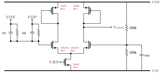
Figure 22: The common mode feedback amplifier. VON and VOP are sensed through 60k||20f networks and compared against a 100k/100k mid-supply reference. Each load PMOS is diode connected on its own - the gates are not tied together - so the gain is the modest, well defined $g_{mn}/g_{mp}$ that a common mode loop wants, and the correction leaves as $V_{CMFB}$
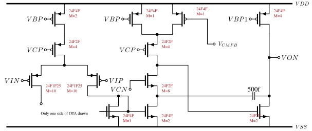
Figure 23: The OTA itself, one side drawn, sized in multiples of the minimum gate length F: a cascoded PMOS tail into the input pair, a cascoded mirror making the first stage output, and a common source second stage with 500 fF of cascode compensation. $V_{CMFB}$ arrives from the amplifier in Figure 13
As bias circuit to make the voltages the below will work
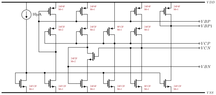
Figure 24: The bias generator. The 10 uA reference is mirrored once in an ordinary current mirror - the line along the bottom - and everything above it is wide swing cascode: the narrow 8F12F devices set VCP and VCN, and in each master the mirror device’s gate hangs on the far end of its own stack
Switches
If your gut reaction is “switches, that’s easy”, then you’re very wrong. Switches can be incredibly complicated. All switches will be made of transistors, but usually we don’t have enough headroom to use a single NMOS or PMOS. We may need a transmission gate
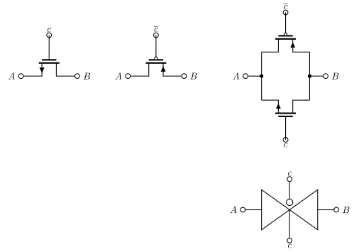
Figure 25: Switch implementations: NMOS, PMOS, transmission gate, and the transmission gate symbol
The challenge with transmission gates is that when the voltage at the input is in the middle between VDD and ground then both PMOS and NMOS, although they are on , they might not be that on. Especially in nano-scale CMOS with a 0.8 V supply and 0.5 V threshold voltage. The resistance mid-rail might be too large.
For switched-capacitor circuits we must settle the voltages to the required accuracy. In general
\[t > -\ln(\text{error} ) \tau\]For example, for a 10-bit ADC we need $t > -\ln(1/1024) \tau = 6.9\tau$. This means we need to wait at least 6.9 time constants for the voltage to settle to 10-bit accuracy in the switched capacitor circuit.
Assume the capacitors are large due to noise, then the switches must be low resistance for a reasonable time constant. Larger switches have smaller resistance, however, they also have more charge in the inversion layer, which leads to charge injection when the switches are turned off. Accordingly, larger switches are not always the solution.
Sometimes it may be sufficient to switch the bulks, as shown on the left below. But more often than one would like, we have to implement bootstrapped switches as shown on the right.
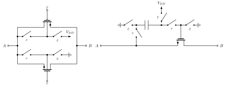
Figure 26: Transmission gate with switched bulks (left) and a bootstrapped switch (right)
The switch I used in my JSSC SAR 5 is a fully differential bootstrapped switch with cross coupled dummy transistors. The JSSC SAR I’ve also ported to GF130NM, as shown below. The switch is at the bottom.
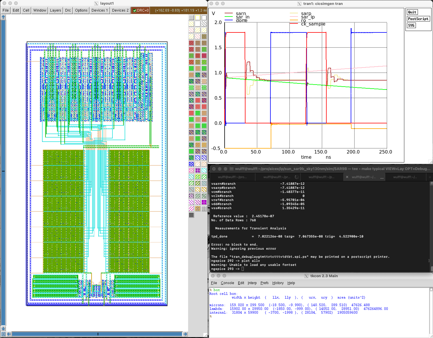
Figure 27: Layout and transient simulation of the 9-bit SAR ADC, with the bootstrapped sampling switch at the bottom
The bootstrapped switch looks like the one below.
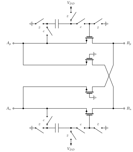
Figure 28: Fully differential bootstrapped switch with cross coupled dummy transistors
Non-overlapping clocks
Everything in this chapter has rested on charge going exactly where we said it goes. That holds only if the two phases are never on at the same time. Overlap them, even briefly, and a path opens from the input straight through to the summing node while the previous charge is still there: some charge escapes, some arrives early, and the gain is no longer $C_1/C_2$ but something that depends on how long the overlap lasted. It is a gain error that changes with temperature and corner, which is the worst kind.
The generator below solves this the obvious way. Each phase is fed back to the gate of the other’s driver, so neither can rise until the other has fallen, and the delay chain sets how much dead time sits between them. The cost is that dead time — clock period you are not using — so it wants to be sufficient and no more.
Sufficient in all corners, though. The delay chain is made of inverters, and the ring oscillator plots earlier in the logic chapter show what happens to inverter delay across process and temperature: it moves by a factor of two or three. Simulate the non-overlap at the fast corner, where it is smallest, not at typical.
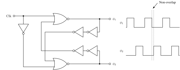
Figure 29: Non-overlapping clock generator and the resulting phases $\phi_1$ and $\phi_2$
Example
In the circuit below there is an example of a switched capacitor circuit used to increase the $\Delta V_{D}$ across the resistor. We can accurately set the gain, and thus the equation for the differential output will be
\[V_O(z) = 10 \frac{kT}{q} \ln (N)z^{-1}\]Every factor in that expression comes from somewhere earlier, and it is worth naming them, because this one circuit is most of the course so far in a single schematic.
The $\frac{kT}{q}\ln(N)$ is the PTAT difference between two diode voltages at a current ratio $N$, from the references chapter. It is small, a few tens of millivolts, and it is proportional to absolute temperature, which is what makes it useful as a temperature signal.
The $10$ is $C_1/C_2$, a capacitor ratio, from this chapter. That is the whole reason for doing the amplification this way: a capacitor ratio in one piece of silicon matches to a fraction of a percent, so the gain is accurate in a way a resistor ratio or a transistor parameter would not be, and it does not drift with temperature.
The $z^{-1}$ is one clock period of delay, because the charge sampled in phase 1 does not reach the output until phase 2.
So the circuit takes a signal defined by physical constants, multiplies it by a number defined by geometry, and delivers the result one clock later. Nothing in the answer depends on a transistor’s threshold voltage, its mobility, or the supply. That is the point of switched capacitor circuits, and it is why they survived into processes where almost nothing else about analog design got easier.
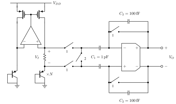
Figure 30: Switched capacitor amplifier scaling the bipolar generated voltage by $C_1/C_2 = 10$
Summary
The one-page version of this chapter:
- A switched capacitor is a resistor R = 1/(f C) made of ratio-accurate parts: SC filters get their time constants from C ratios and a clock
- Sampling moves the world to discrete time: the z-domain, aliasing and the sample-rate theorem come with it
- The parasitic-insensitive integrator and the SC gain stage are the two workhorse circuits; correlated double sampling throws in offset removal
- Every sample costs kT/C of noise - capacitor sizes come from the noise budget, not the layout
- Switches need non-overlapping clocks, and bootstrapping when the signal swings
- Behind every SC circuit stands an OTA and its bias; the settling budget is half a clock period, verified in the transient
Would you like to know more?
Blind Multiband Signal Reconstruction: Compressed Sensing for Analog Signal 3
Comparator-based switched-capacitor pipelined analog-to-digital converter with comparator preset, and comparator delay compensation 4
A Compiled 9-bit 20-MS/s 3.5-fJ/conv.step SAR ADC in 28-nm FDSOI for Bluetooth Low Energy Receivers 5
A 10-bit 50-MS/s SAR ADC With a Monotonic Capacitor Switching Procedure 6
Low Voltage, Low Power, Inverter-Based Switched-Capacitor Delta-Sigma Modulator 7
Ring Amplifiers for Switched Capacitor Circuits 8
A Switched-Capacitor RF Power Amplifier 9
Design of Active N-Path Filters 10
-
I use the $ to mark the end of the period. It comes from Regular Expressions. ↩
-
S.H. Lewis and P.R. Gray, A pipelined 5-Msample/s 9-bit analog-to-digital converter 1987 ↩ ↩2
-
M. Mishali and Y. C. Eldar, Blind Multiband Signal Reconstruction: Compressed Sensing for Analog Signals 2009 https://doi.org/10.1109/TSP.2009.2012791 ↩ ↩2
-
C. Wulff and T. Ytterdal, Comparator-based switched-capacitor pipelined analog-to-digital converter with comparator preset, and comparator delay compensation 2010 https://doi.org/10.1007/s10470-010-9576-3 ↩ ↩2
-
Wulff, Carsten and Ytterdal, Trond, A Compiled 9-bit 20-MS/s 3.5-fJ/conv.step SAR ADC in 28-nm FDSOI for Bluetooth Low Energy Receivers 2017 https://doi.org/10.1109/JSSC.2017.2685463 ↩ ↩2
-
C. C. Liu and S. J. Chang and G. Y. Huang and Y. Z. Lin, A 10-bit 50-MS/s SAR ADC With a Monotonic Capacitor Switching Procedure 2010 https://doi.org/10.1109/JSSC.2010.2042254 ↩
-
Y. Chae and G. Han, Low Voltage, Low Power, Inverter-Based Switched-Capacitor Delta-Sigma Modulator 2009 https://doi.org/10.1109/JSSC.2008.2010973 ↩
-
B. Hershberg and S. Weaver and K. Sobue and S. Takeuchi and K. Hamashita and U.-K. Moon, Ring Amplifiers for Switched Capacitor Circuits 2012 https://doi.org/10.1109/JSSC.2012.2217865 ↩
-
S.-M. Yoo and J. S. Walling and E. C. Woo and B. Jann and D. J. Allstot, A Switched-Capacitor RF Power Amplifier 2011 https://doi.org/10.1109/JSSC.2011.2163469 ↩
-
M. Darvishi and R. van der Zee and B. Nauta, Design of Active N-Path Filters 2013 https://doi.org/10.1109/JSSC.2013.2285852 ↩