Table of contents
Keywords:
Processing of signals has shifted into the digital domain. But the real world is analog. In order to interact with the analog we need to convert the digital signals (discrete-value, discrete-time) back to analog signals (continuous value, continuous time).
The SI base units define the fundamental analog quantities as second, meter, kilogram, ampere, kelvin, mole and candela (see the refresher). Assume that electronic circuits interact with the real world in terms of second and ampere.
Related to Ampere we have the derived units of charge (Ampere Seconds), Volt (W/A), Ohm (V/A), or indeed Siemens (1/$\Omega$).

Figure 1: NIST poster of the SI base units and the derived units. Image: NIST, US Department of Commerce (US federal work)
As such, to create a digital to analog converter, we somehow have to create a circuit that has a function of
\[I_{out} = D_{in} \times I_{ref}\text{ [I]}\] \[t_{out} = D_{in} \times t_{ref}\text{ [s]}\] \[Q_{out} = D_{in} \times Q_{ref}\text{ [C]}\] \[V_{out} = D_{in} \times V_{ref}\text{ [V]}\] \[R_{out} = D_{in} \times R_{ref}\text{ [}\Omega\text{]}\]The digital value is dimensionless, as such, there must be a reference value
Digital to analog conversion can be indirect through the relations between voltage, resistance, current, time, inductance and capacitance.
\[V = R I\] \[Q = C V\] \[dt = \frac{C dV}{I}\] \[dt = \frac{L dI}{V}\]Resistor based DACs
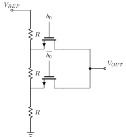
Figure 2: 1-bit DAC: three series resistors with transistor switches selecting the output tap
\[I_{ref} = \frac{V_{ref}}{3 R}\] \[V_{out} = D_{in} R I_{ref} = \frac{D_{in} R V_{ref}}{3 R} \text{ [V]}\] \[V_{out} = \frac{b_0 2 R V_{ref}}{3 R} + \frac{\overline{b_0} R V_{ref}}{3 R}\] \[V_{out} = \begin{cases} \frac{2}{3} V_{ref}, & b_0 = 1 \\ \frac{1}{3} V_{ref}, & b_0 = 0 \end{cases}\]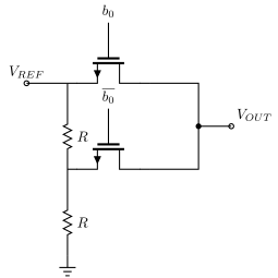
Figure 3: 1-bit DAC with two resistors, selecting either $V_{REF}$ or the midpoint
\[I_{ref} = \frac{V_{ref}}{2 R}\] \[V_{out} = \frac{b_0 2 R V_{ref}}{2 R} + \frac{\overline{b_0} R V_{ref}}{2 R}\] \[V_{out} = \begin{cases} V_{ref}, & b_0 = 1 \\ \frac{1}{2} V_{ref}, & b_0 = 0 \end{cases}\]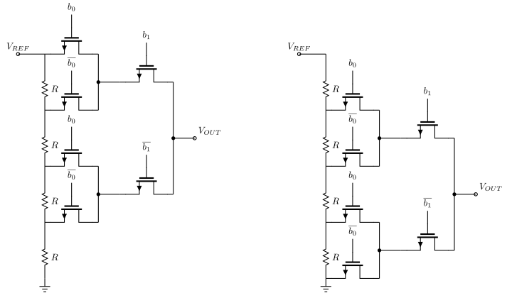
Figure 4: Two possible 2-bit resistor string DACs with switch trees
DAC errors
Digital to analog converters do not add quantization error. The quantization error is already in the digital word.
\[V_{out} = B + a_1 D_{in} + \left( a_2 D_{in}^2 + \dots + a_n D_{in}^n \right)\]Read that as three separate defects. $B$ is offset, a constant added to every code. $a_1$ is gain, which stretches the transfer curve but keeps it straight. Everything in the bracket is non-linearity, and it is the only part that a calibration of gain and offset cannot remove.
DAC output will contain gain errors, offset errors, and non-linear components
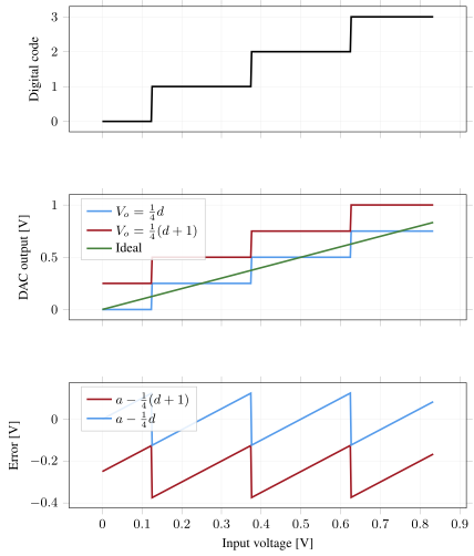
Figure 5: Quantization error of a 2-bit DAC. The digital code (top), two conventions for turning that code back into a voltage (middle), and the error each one makes (bottom)
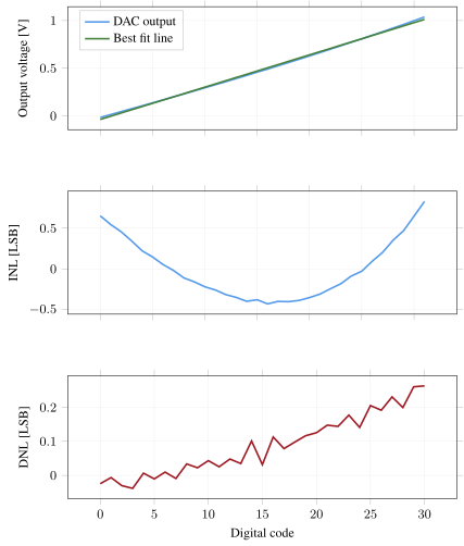
Figure 6: DAC output compared to the ideal straight line, with INL and DNL versus digital code
\[DNL[k] = \frac{V[k+1] - V[k]}{V_{LSB}} - 1\] \[INL[k] = \frac{V[k] - V_{ideal}[k]}{V_{LSB}}\]DAC complexity
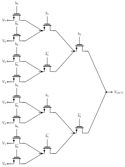
Figure 7: Binary switch tree for a resistor string DAC
The resistor string itself is the easy part - $2^N$ equal resistors give $2^N$ perfectly ordered taps, and the DAC is monotonic by construction. The cost hides in the selection: something must connect exactly one tap to the output. The obvious structure is a binary tree, where each bit steers a rank of switches, and the count below says why nobody stops there.
As number of resistors grow, the switches grow as
\[\sum_{n=1}^{N} 2^n = 2^{N+1} - 2\]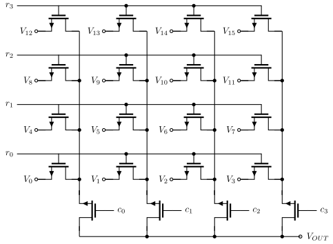
Figure 8: Row and column switch matrix for a resistor string DAC
The matrix halves the damage by decoding in two dimensions, the way a memory does: the row decoder picks a group of taps, the column switches pick one of them. The tap switches are still there - they must be, every tap has to be reachable - but the tree above them collapses into one switch per column.
Give every tap a switch onto a column line, and every column line a switch to the output. For $2^N$ taps in a square arrangement that is
\[2^{N} + 2^{N/2}\]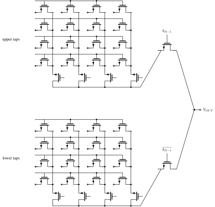
Figure 9: Segmented DAC switch arrangement combining switch matrices and a tree
Switches in a 10-bit digital to analog converter.
\[\begin{array}{lll} \text{Tree} & 2^{N+1}-2 & = 2046 \\ \text{Matrix} & 2^{N} + 2^{N/2} & = 1056 \\ \text{Two strings, 6b + 4b} & 2^{M} + 2^{N-M} & = 80 \\ \text{Two strings, 5b + 5b} & 2^{M} + 2^{N-M} & = 64 \end{array}\]Those three lines are not three versions of the same circuit, and the difference between the first two and the last is the point of this section.
The tree and the matrix both address one string of $2^N$ resistors, so both need at least one switch per tap. The tree adds switches at every internal node on top of that, which is why it is the worst of the three; the matrix adds only one per column, which is why it is roughly half the tree. Neither can go below $2^N$, because every tap has to be reachable on its own.
It is worth being clear that combining them does not help. A tree of matrix blocks — a plausible reading of the figure above — still needs its $2^N$ tap switches and now pays for the tree as well: a 4-bit tree over sixteen 6-bit matrices comes to 1182, worse than the plain matrix at 1056. Every split is worse. There is nothing to win by decoding the same string more cleverly.
The saving comes from not having one string at all. Put a coarse string of $2^M$ resistors in series and let a fine string of $2^{N-M}$ resistors interpolate between two adjacent coarse taps, and each selector only has to reach its own string: $2^M + 2^{N-M}$ switches rather than $2^N$. For ten bits split six and four that is 80, and the best split is five and five at 64 — against 1056 for the matrix. Trading one big decoder for two small ones is worth a factor of sixteen here, and the reason is simply that $2^M + 2^{N-M}$ grows far more slowly than $2^N$.
Nothing is free: the fine string loads the coarse one and disturbs the very voltage it is interpolating, a real two-string DAC needs a second switch per coarse tap to bracket the segment, and the matching now has to hold between two strings rather than within one. But the switch count is no longer what stops you.
Large number of bits, will be large number of resistors and switches.
Binary scaled DACs
A string DAC pays $2^N$ resistors for $N$ bits. The R-2R ladder pays $2N$: each section divides the remaining voltage by two, so the branch currents come out binary weighted with only two resistor values. The next four figures build the ladder one property at a time - the termination, the input resistance that stays 2R at every section, and the halving branch currents that make it a DAC.
\[R_{in} = 2R \parallel 2R = R\]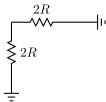
Figure 10: R-2R ladder termination: two 2R resistors in parallel equal R
\[R_{in} = R + R = 2R\] \[I_{0} = \frac{V_0}{2R} = \frac{V_1}{4R}\]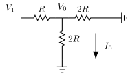
Figure 11: One R-2R ladder section: the series R makes the input resistance 2R
\[R_{in} = 2R \parallel 2R = R\] \[I_{0} = \frac{V_0}{2R} = \frac{V_1}{4R}\] \[I_{1} = \frac{V_1}{2R}\]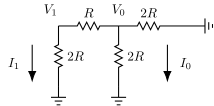
Figure 12: R-2R ladder section with the binary weighted branch currents $I_1$ and $I_0$
\[I_{RF} = I_1b_1 + I_0b_0 = \frac{V_{REF}}{2R}b_1 + \frac{V_{REF}}{4R}b_0\] \[V_{O} = \left(\frac{V_{REF}}{2R}b_1 + \frac{V_{REF}}{4R}b_0\right)R_{F0}\]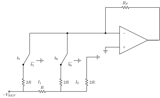
Figure 13: 2-bit R-2R DAC with switched branch currents summed by a transimpedance amplifier
The switches steer each branch current either into the virtual ground of the amplifier or to real ground, so the ladder’s currents never change - only their destination does. That is what makes the R-2R fast for its size. What it gives up is the string’s built-in monotonicity: at the major transition the MSB branch must match the sum of all the others to within an LSB, and that is now a matching requirement on the resistors rather than a property of the structure.
Binary coding
For 4 states (2-bit) there are 12 possible transitions
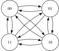
Figure 14: The 12 possible transitions between the four 2-bit binary states
Assume MSB first (left)
\[1 \rightarrow 3 \rightarrow 2\]Assume LSB first (right)
\[1 \rightarrow 0 \rightarrow 2\]Both cause a non-monotonic glitch during transition.
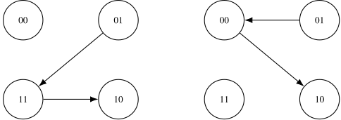
Figure 15: Binary code transitions with MSB first (left) and LSB first (right), both non-monotonic
The switches never move at exactly the same time. Between the old code and the new one the DAC output visits whatever code the half-switched bits happen to spell, and around the major transition - 0111 to 1000 - that intermediate code can be far away. The result is a glitch whose energy grows with the weight of the bits involved, and no amount of matching removes it: it is a property of the code, not of the elements.
Thermometer encoding
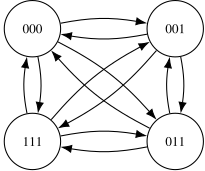
Figure 16: Transitions between the thermometer encoded states
The sequence of MSB to LSB does not matter.
\[0 \rightarrow 1 \rightarrow 2 \rightarrow 3\]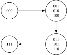
Figure 17: Thermometer code transitions are monotonic regardless of bit order
Thermometer coding removes the glitch by construction: one more LSB always means one more element turned on, so the output can only move one step, whatever order the switches settle in. Monotonicity comes for free for the same reason. The price is $2^N - 1$ elements and the decoder that drives them, which is why real converters segment - thermometer for the MSBs where the glitch would be worst, binary for the LSBs where it cannot hurt.
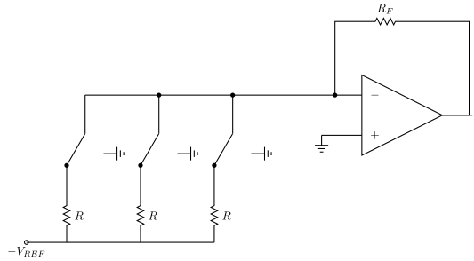
Figure 18: Thermometer coded resistor DAC with equal resistors summed by a transimpedance amplifier
Current mode DACs
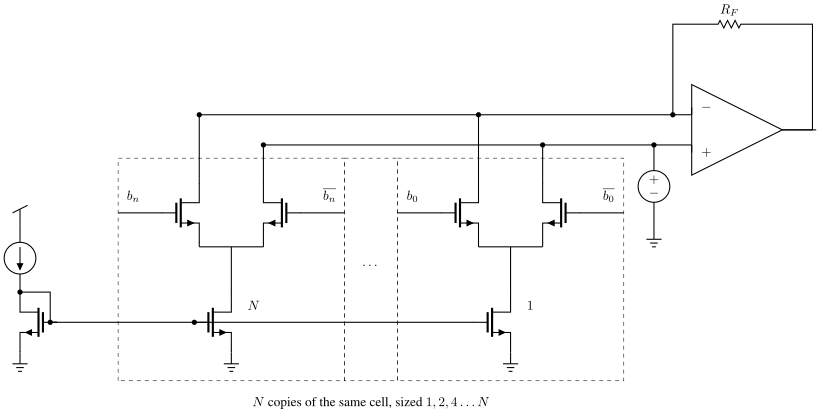
Figure 19: Current mode DAC: binary sized differential current cells switched into a transimpedance output stage
At high sample rates the resistor structures run out of settling time, and the current steering DAC takes over: every cell is a current source that is always on, and the data only chooses which side of a differential pair the current leaves through. Nothing charges or discharges except the switch nodes, so this is the architecture behind every GS/s transmitter DAC.
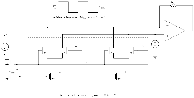
Figure 20: Current mode DAC where the switch drive swings around $V_{bias}$ instead of rail to rail
Driving the steering pair rail to rail briefly turns both switches off and slams the source node; the cell’s current has to go somewhere, and it goes into the output as a spike. Limiting the switch drive to a small swing around $V_{bias}$ keeps the pair in its active region through the crossover, keeps the current source in saturation, and is the difference between a DAC that meets its SFDR and one that only meets its resolution.
Summary
The one-page version of this chapter:
- A DAC turns a code into charge, current or voltage by summing weighted unit elements
- Binary weighting is compact but must switch half the array at the major carry; thermometer coding is monotonic and glitch-free but costs 2^N elements and decoding
- Segmentation spends thermometer coding on the MSBs where it matters and binary on the LSBs where it is cheap
- Static accuracy is INL/DNL set by element matching (Pelgrom: area buys bits); dynamic accuracy is glitch energy and SFDR
- The references and the switch drivers are part of the DAC: their noise and timing skew show up in the output spectrum
Would you like to know more?
A 28-nm 75-fsrms Analog Fractional-N Sampling PLL With a Highly Linear DTC Incorporating Background DTC Gain Calibration and Reference Clock Duty Cycle Correction [^1]
A 10-bit Charge-Redistribution ADC Consuming 1.9 uW at 1 MS/s [^2]
A 6.3 uW 20 bit Incremental Zoom-ADC with 6 ppm INL and 1 uV Offset [^3]
A 12-Bit 1.25-GS/s DAC in 90 nm CMOS With >70 dB SFDR up to 500 MHz [^4] [^1]: W. Wu and C.-W. Yao and K. Godbole and R. Ni and P.-Y. Chiang and Y. Han and Y. Zuo and A. Verma and I.-S.-C. Lu and S. W. Son and T. B. Cho, A 28-nm 75-fsrms Analog Fractional- $N$ Sampling PLL With a Highly Linear DTC Incorporating Background DTC Gain Calibration and Reference Clock Duty Cycle Correction 2019 https://doi.org/10.1109/JSSC.2019.2899726 [^2]: M. van Elzakker and E. van Tuijl and P. Geraedts and D. Schinkel and E. A. M. Klumperink and B. Nauta, A 10-bit Charge-Redistribution ADC Consuming 1.9 $\mu$W at 1 MS/s 2010 https://doi.org/10.1109/JSSC.2010.2043893 [^3]: Y. Chae and K. Souri and K. A. A. Makinwa, A 6.3 $\mu$W 20 bit Incremental Zoom-ADC with 6 ppm INL and 1 $\mu$V Offset 2013 https://doi.org/10.1109/JSSC.2013.2278737 [^4]: W.-H. Tseng and C.-W. Fan and J.-T. Wu, A 12-Bit 1.25-GS/s DAC in 90 nm CMOS With $ > $70 dB SFDR up to 500 MHz 2011 https://doi.org/10.1109/JSSC.2011.2164302