Table of contents
Keywords: Systems, Feedback, PLL, Integer Divider, SD, SD PLL, Modulation, linear phase model
Why clocks?
Virtually all integrated circuits have some form of clock system.
For digital we need clocks to tell us when the data is correct. For Radio’s we need clocks to generate the carrier wave. For analog we need clocks for switched regulators, ADCs, accurate delay’s or indeed, long delays.
The principle of a clock is simple. Make a 1-bit digital signal that toggles with a period $T$ and a frequency $f = 1/T$.
The implementation is not necessarily simple.
The key parameters of a clock are the frequency of the fundamental, noise of the frequency spectrum, and stability over process and enviromental conditions.
When I start a design process, I want to know why, how, what (and sometimes who). If I understand the problem from first principles it’s more likely that the design will be suitable.
But proving that something is suitable, or indeed optimal, is not easy in the world of analog design. Analog design is similar to physics. An hypothesis is almost impossible to prove “correct”, but easier to prove wrong.
A customer story
Take an example.
Imagine a world
“I have a customer that needs an accurate clock to count seconds”. – Some manager that talked to a customer, but don’t understand details.
As a designer, I might latch on to the word “accurate clock”, and translate into “most accurate clock in the world”, then I’d google atomic clocks, like Rubidium standard that I know is based on the hyperfine transition of electrons between two energy levels in rubidium-87.
I know from quantum mechanics that the hyperfine transition between two energy levels will produce an precise frequency, as the frequency of the photons transmitted is defined by $E = \hbar \omega = h f$.
I also know that quantum electro dynamics is the most precise theory in physics, so we know what’s going on.
As long as the Rubidium crystal is clean (few energy states in the vicinity of the hyperfine transition), the distance between atoms stay constant, the temperature does not drift too much, then the frequency will be precise. So I buy a rubidium oscillator at a cost of $ 3k.
I design an ASIC to count the clock ticks, package it plastic, make a box, and give my manager.
Who will most likely say something like
“Are you insane? The customer wants to put the clock on a wristband, and make millions. We can’t have a cost of $ 3k per device. You must make it smaller and it must cost 10 cents to make”
Where I would respond.
“What you’re asking is physically impossible. We can’t make the device that cheap, or that small. Nobody can do that.”
And both my manager and I would be correct.
Imagine a better world
Most people in this world have no idea how things work. Very few people are able to understand the full stack. Everyone of us must simplify what we know to some extent. As such, as a circuit designer, it’s your responsibility to fully understand what is asked of you.
When someone says
” I have a customer that needs an accurate clock to count seconds”
Your response should be “Why does the customer need an accurate clock? How accurate? What is the customer going to use the clock for?”. Unless you understand the details of the problem, then your design will be sub-optimal. It might be a great clock source, but it will be useless for solving the problem.
Frequency
The frequency of the clock is the frequency of the fundamental. If it’s a digital clock (1-bit) with 50 % duty-cycle, then we know that a digital pulse train is an infinite sum of odd harmonics, where the fundamental is given by the period of the train.
Noise
Clock noise have many names. Cycle-to-cycle jitter is how the period changes with time. Jitter may also mean how the period right now will change in the future, so a time-domain change in the amount of cycle-to-cycle jitter. Phase noise is how the period changes as a function of time scales. For example, a clock might have fast period changes over short time spans, but if we average over a year, the period is stable.
What type of noise you care about depends on the problem. Digital will care about the cycle-to-cycle jitter affects on setup and hold times. Radio’s will care about the frequency content of the noise with an offset to the carrier wave.
Stability
The variation over all corners and enviromental conditions is usually given in a percentage, parts per million, or parts per billion.
For a digital clock to run a Micro-Controller, maybe it’s sufficient with 10% accuracy of the clock frequency. For a Bluetooth radio we must have +-50 ppm, set by the standard. For GPS we might need parts-per-billion.
Conclusion
Each “clock problem” will have different frequency, noise and stability requirements. You must know the order of magnitude of those before you can design a clock source. There is no “one-solution fits all” clock generation IP.
A typical System-On-Chip clock system
On the nRF52832 development kit you can see some components that indicate what type of clock system must be inside the IC.
In the figure below you can see the following items.
- 32 MHz crystal
- 32 KiHz crystal
- PCB antenna
- DC/DC inductor
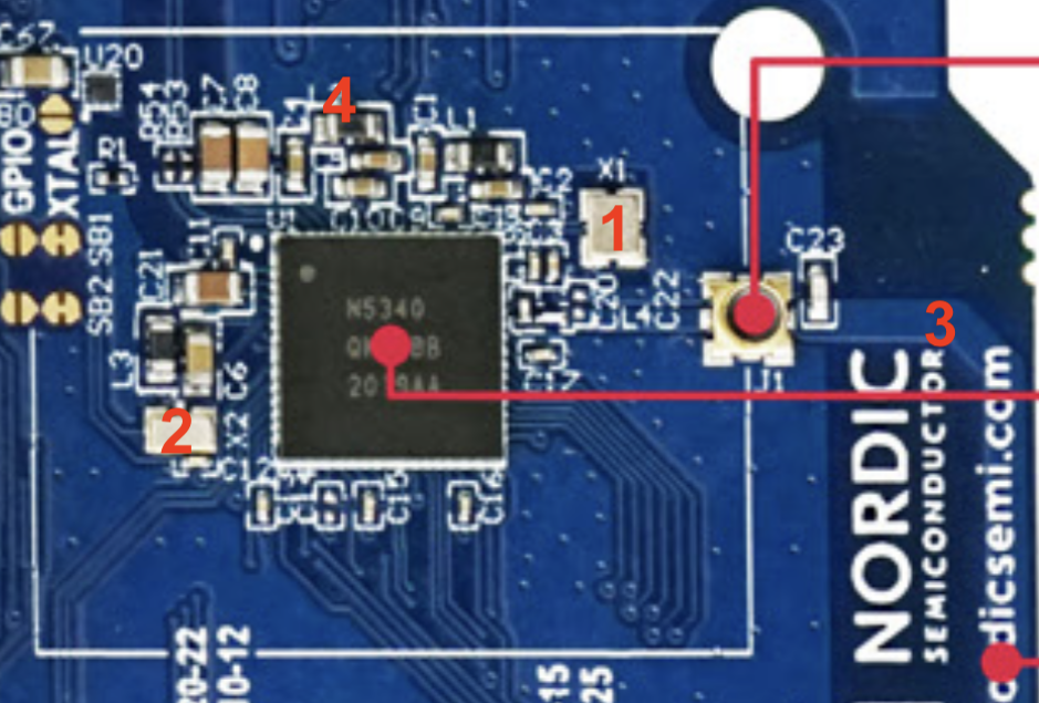
Figure 1: nRF5 development kit PCB with (1) 32 MHz crystal, (2) 32 KiHz crystal, (3) PCB antenna, and (4) DC/DC inductor. Source: Nordic Semiconductor, nRF5340 documentation
32 MHz crystal
Any Bluetooth radio will need a frequency reference. We need to generate an accurate 2.402 GHz - 2.480 GHz carrier frequency for the gaussian frequency shift keying (GFSK) modulation. The Bluetooth Standard requires a +- 50 ppm accurate timing reference, and carrier frequency offset accuracy.
I’m not sure it’s possible yet to make an IC that does not have some form of frequency reference, like a crystal. The ICs I’ve seen so far that have “crystal less radio” usually have a resonator (crystal or bulk-acoustic-wave or MEMS resonator) on die.
The power consumption of a high frequency crystal will be proportional to frequency. Assuming we have a digital output, then the power of that digital output will be $P = C V^2 f$, for example $P = 100\text{ fF} \times 1\text{ V}^2 \times 32\text{ MHz} = 3.2\text{ } \mu\text{W}$ is probably close to a minimum power consumption of a 32 MHz clock.
32 KiHz crystal
Reducing the frequency, we can get down to minimum power consumption of $P = 100\text{ fF} \times 1\text{ V}^2 \times 32\text{ KiHz} = 3.2 \text{ nW}$ for a clock.
For a system that sleeps most of the time, and only wakes up at regular ticks to do something, then a low-frequency crystal might be worth the effort.
PCB antenna
Since we can see the PCB antenna, we know that the IC includes a radio. From that fact we can deduce what must be inside the SoC. If we read the Product Specification we can understand more.
DC/DC inductor
Since we can see a large inductor, we can also make the assumption that the IC contains a switched regulator. That switched regulator, especially if it has a pulse-width-modulated control loop, will need a clock.
From our assumptions we could make a guess what must be inside the IC, something like the picture below.
There will be a crystal oscillator connected to the crystal. We’ll learn about those later.
These crystal oscillators generate a fixed frequency, 32 MHz, or 32 KiHz, but there might be other clocks needed inside the IC.
To generate those clocks, there will be phase-locked loops (PLL), frequency locked loops (FLL), or delay-locked loops (DLL).
PLLs take a reference input, and can generate a higher frequency, (or indeed lower frequency) output. A PLL is a magical block. It’s one of the few analog IPs where we can actually design for infinite gain in our feedback loop.
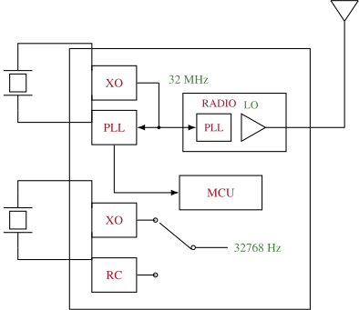
Figure 2: Guess at the clock system inside the SoC: crystal oscillators (XO) for 32 MHz and 32768 Hz, a PLL for the radio local oscillator, an RC oscillator, and the MCU clock
Most of the digital blocks on an IC will be synchronous logic, see figure below. A fundamental principle of synchronous logic is that the data at the flip-flops (DFF, rectangles with triangle clock input, D, Q and $\overline{\text{Q}}$) only need to be correct at certain times.
The sequence of transitions in the combinatorial logic is of no consequence, as long as the B inputs are correct when the clock goes high next time.
The registers, or flip-flops, are your SystemVerilog “always_ff” code. While the blue cloud is your “always_comb” code.
In a SoC we have to check, for all paths between a Y[N] and B[M] that the path is fast enough for all transients to settle before the clock strikes next time. How early the B data must arrive in relation to the clock edge is the setup time of the DFFs.
We also must check for all paths that the B[M] are held for long enough after the clock strikes such that our flip-flop does not change state. The hold time is the distance from the clock edge to where the data is allowed to change. Negative hold times are common in DFFs, so the data can start to change before the clock edge.
In an IC with millions of flip-flops there can be billions of paths. The setup and hold time for every single one must be checked. One could imagine a simulation of all the paths on a netlist with parasitics (capacitors and resistors from layout) to check the delays, but there are so many combinations that the simulation time becomes unpractical.
Static Timing Analysis (STA) is a light-weight way to check all the paths. For the STA we make a model of the delay in each cell (captured in a liberty file), the setup/hold times of all flip-flops, wire propagation delays, clock frequency (or period), and the variation in the clock frequency. The process, voltage, temperature variation must also be checked for all components, so the number of liberty files can quickly grow large.
For an analog designer the constraints from digital will tell us what’s the maximum frequency we can have at any point in time, and what is the maximum cycle-to-cycle variation in the period.
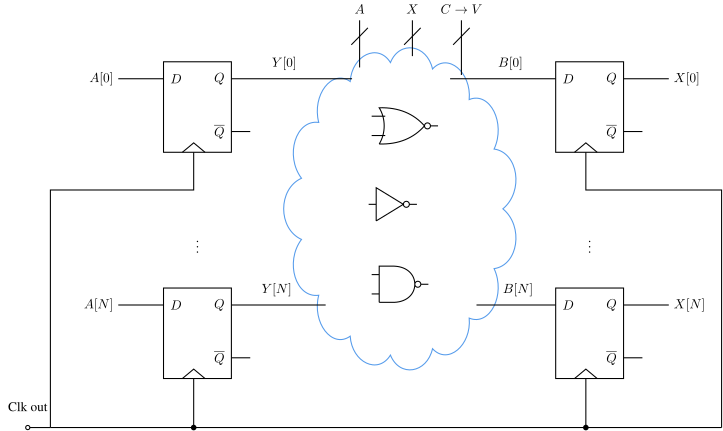
Figure 3: Synchronous logic: flip-flops capture the data on the clock edge, with combinatorial logic (blue cloud) between register stages
PLL
PLL, or it’s cousins FLL and DLL are really cool. A PLL is based on the familiar concept of feedback, shown in the figure below. As long as we make $H(s)$ infinite we can force the output to be an exact copy of the input.
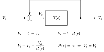
Figure 4: Feedback loop where an infinite gain H(s) forces the output to be an exact copy of the input
Integer PLL
For a frequency loop the figure looks a bit different. If we want a higher output frequency we can divide the frequency by a number (N) and compare with our reference (for example the 32 MHz reference from the crystal oscillator).
We then take the error, apply a transfer function $H(s)$ with high gain, and control our oscillator frequency.
If the down-divided output frequency is too high, we force the oscillator to a lower frequency. If the down-divided output frequency is too low we force the oscillator to a higher frequency.
If we design the $H(s)$ correctly, then we have $f_o = N \times f_{in}$
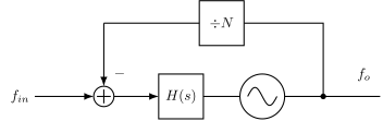
Figure 5: Integer PLL: the oscillator output is divided by N and compared to the reference, giving an output frequency N times the reference
Sometimes you want a finer frequency resolution, in that case you’d add a divider on the reference and get $f_o = N \times \frac{f_{in}}{M}$..
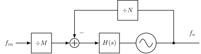
Figure 6: Integer PLL with an additional divide-by-M on the reference for finer frequency resolution
Fractional PLL
Trouble is that dividing down the input frequency will reduce your loop bandwidth, as the low-pass filter needs to be about 1/10’th of the reference frequency. As such, the PLL will respond slower to a frequency change.
We can also use a fractional divider, where we swap between two, or more, integers in a sigma-delta fashion in the divider.
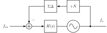
Figure 7: Fractional PLL where a sigma-delta modulator switches the feedback divider between integer values
Modulation in PLLs
From your signal processing, or communication courses, you may recognize the equation below.
\[A_m(t) \times cos\left( 2 \pi f_{carrier}t + \phi_{m}(t)\right)\]The $A_m$ is the amplitude modulation, while the $\phi_m$ is the phase modulation. Bluetooth Low Energy is constant envelope, so the $A_m$ is a constant. The phase modulation is applied to the carrier, but how is it done?
One option is shown below. We could modulate our frequency reference directly. That could maybe be a sigma-delta divider on the reference, or directly modulating the oscillator.
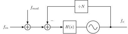
Figure 8: Modulating the PLL by adding the modulation signal directly to the frequency reference
Most modern radios, however, will have a two-point modulation. The modulation signal is applied to the VCO (or DCO), and the opposite signal is applied to the feedback divider. As such, the modulation is not seen by the loop.
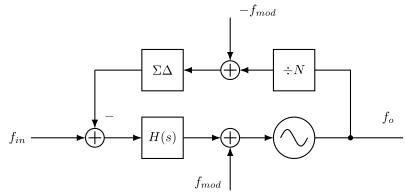
Figure 9: Two-point modulation: the modulation is applied to the oscillator and the opposite signal to the sigma-delta feedback divider, so the loop does not see it
PLL Example
I’ve made an example PLL that you can download and play with. I make no claims that it’s a good PLL. Actually, I know it’s a bad PLL. The ring-oscillator frequency varies too fast with the voltage control. But it does give you a starting point.
A PLL can consist of a oscillator (SUN_PLL_ROSC) that generates our output frequency. A divider (SUN_PLL_DIVN) that generates a feedback frequency that we can compare to the reference. A Phase and Frequency Detector (SUN_PLL_PFD) and a charge-pump (SUN_PLL_CP) that model the $+$, or the comparison function in our previous picture. And a loop filter (SUN_PLL_LPF and SUN_PLL_BUF) that is our $H(s)$.
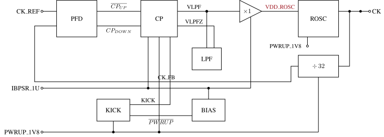
Figure 10: Top-level schematic of the SUN_PLL example with phase-frequency detector, charge-pump, loop filter, buffer, ring oscillator, and divide-by-32 feedback divider. Block placement follows the xschem source: signal flow left to right along the loop, feedback below, bias and start-up at the bottom
Read any book on PLLs, talk to any PLL designer and they will all tell you the same thing. PLLs require calculation. You must setup a linear model of the feedback loop, and calculate the loop transfer function to check the stability, and the loop gain. This is the way! (to quote Mandalorian).
But how can we make a linear model of a non-linear system? The voltages inside a PLL must be non-linear, they are clocks. A PLL is not linear in time-domain!
I have no idea who first thought of the idea, but it turns out, that one can model a PLL as a linear system if one consider the phase of the voltages inside the PLL, especially when the PLL is locked (phase of the output and reference is mostly aligned). Where the phase is defined as
\[\phi(t) = 2 \pi \int_0^t f(\tau) d\tau\]As long as the bandwidth of the $H(s)$ is about $\frac{1}{10}$ of the reference frequency, then the linear model below holds (at least is good enough).
The phase of our input is $\phi_{in}(s)$, the phase of the output is $\phi(s)$, the divided phase is $\phi_{div}(s)$ and the phase error is $\phi_d(s)$.
The $K_{pd}$ is the gain of our phase-frequency detector and charge-pump. The $K_{lp}H_{lp}(s)$ is our loop filter $H(s)$. The $K_{osc}/s$ is our oscillator transfer function. And the $1/N$ is our feedback divider.
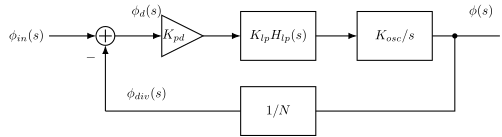
Figure 11: Linear phase-domain model of the PLL with phase-detector gain, loop filter, oscillator integrator and 1/N feedback divider
Loop gain
The loop transfer function can then be analyzed and we get.
\[\frac{\phi_d}{\phi_{in}} = \frac{1}{1 + L(s)}\] \[L(s) = \frac{ K_{osc} K_{pd} K_{lp} H_{lp}(s) }{N s}\]Here is the magic of PLLs. Notice what happens when $s = j\omega = j 0$, or at zero frequency. If we assume that $H_{lp}(s)$ is a low pass filter, then $H_{lp}(0) = \text{constant}$. The loop gain, however, will have a $L(0) \propto \frac{1}{0}$ which approaches infinity at 0.
That means, we have an infinite DC gain in the loop transfer function. It is the only case I know of in an analog design where we can actually have infinite gain. Infinite gain translates to infinite precision.
If the reference was a Rubidium oscillator we could generate any frequency with the same precision as the frequency of the Rubidium oscillator. Magic.
For the linear model, we need to figure out the factors, like $K_{osc}$, which must be determined by simulation.
Controlled oscillator
The gain of the oscillator is the change in output frequency as a function of the change of the control node. For a voltage-controlled oscillator (VCO) we could sweep the control voltage, and check the frequency. The derivative of the f(V) would be proportional to the $K_{vco}$.
The control node does not need to be a voltage. Anything that changes the frequency of the oscillator can be used as a control node. There exist PLLs with voltage control, current control, capacitance control, and digital control.
For the SUN_PLL_ROSC it is the VDD of the ring-oscillator (VDD_ROSC) that is our control node.
\[K_{osc} = 2 \pi\frac{ df}{dV_{cntl}}\]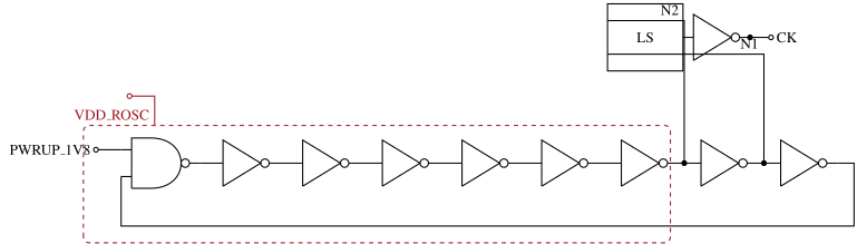
Figure 12: The ring oscillator SUN_PLL_ROSC: a NAND and eight inverters make nine inversions, so the loop oscillates whenever PWRUP_1V8 is high. The ring runs on VDD_ROSC — the supply is the control node — and the level shifter LS brings taps N2/N1 back to the AVDD domain to make CK
SUN_PLL_SKY130NM/sim/ROSC/
I simulate the ring oscillator in ngspice with a transient simulation and get the oscillator frequency as a function of voltage.
tran.spi
let start_v = 1.1
let stop_v = 1.7
let delta_v = 0.1
let v_act = start_v
* loop
while v_act le stop_v
alter VROSC v_act
tran 1p 40n
meas tran vrosc avg v(VDD_ROSC)
meas tran tpd trig v(CK) val='0.8' rise=10 targ v(CK) val='0.8' rise=11
let v_act = v_act + delta_v
end
I use tran.py to extract the time-domain signal from ngspice into a CSV file.
Then I use a python script to extract the $K_{osc}$
kvco.py
    df = pd.read_csv(f)
    freq = 1/df["tpd"]
    kvco = np.mean(freq.diff()/df["vrosc"].diff())
Below I’ve made a plot of the oscillation frequency over corners.
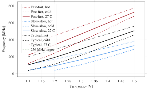
Figure 13: Ring-oscillator frequency versus control voltage VDD_ROSC over nine process and temperature corners, simulated on the extracted layout. The slope at the typical corner is 1.01 GHz/V, which is $K_{osc}$; the spread is a factor of eleven at 1.2 V, narrowing to under three at 1.5 V
Two things in that plot are worth more than the slope.
The first is the spread. A ring oscillator has nothing setting its frequency except how fast its own inverters switch, so process and temperature move it by a factor of eleven at the bottom of the control range. Every corner does cross the 256 MHz the loop needs, but the slow-cold one only at about 1.44 V, near the top of what the control node can deliver. The usable tuning range is not the width of the control range, it is whatever is left above that crossing in the worst corner.
The second is the missing point. At slow-cold and 1.1 V there is no measurement, because the oscillator was too slow to produce enough edges inside the simulated window and the measurement failed rather than returning a plausible wrong number. A failed measurement in the corner you were already worried about is information, not an inconvenience — and it is a good argument for reading the simulator’s errors rather than only its plots.
Phase detector and charge pump
The two blocks compare our reference clock to our feedback clock, and produce an error signal. The gain of the pair is the average current fed into the loop filter per radian of phase error, and it is worth deriving once because the $2\pi$ looks arbitrary until you do.
The phase-frequency detector turns a phase error into a pulse width. If the feedback clock arrives late by a phase $\Delta\phi$, the UP output is high for the fraction $\Delta\phi/2\pi$ of the reference period, because a full period is $2\pi$ of phase. During that pulse the charge pump sources its full current $I_{cp}$, and for the rest of the period it sources nothing. The average current into the filter is therefore
\[\overline{I} = I_{cp}\frac{\Delta\phi}{2\pi}\]and the gain, being average current per radian, is what is left when you divide by $\Delta\phi$:
\[K_{pd} = \frac{I_{cp}}{2 \pi}\]Two things follow that are easy to miss. The gain does not depend on the reference frequency, because both the pulse width and the period scale together. And it is the average current that the loop filter sees, which is only a fair description if the filter is slow compared with the reference — the same assumption that let us draw a linear model in the first place.
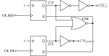
Figure 14: The phase-frequency detector SUN_PLL_PFD: two flip-flops with D tied high, one set by CK_REF, the other by CK_FB. The moment both are set the NOR resets the pair, so the surviving pulse width is the arrival-time difference — phase error becomes pulse width
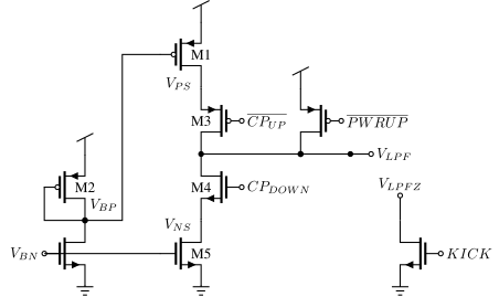
Figure 15: The charge pump SUN_PLL_CP, driven by the phase-frequency detector through CP_UP_N and CP_DOWN. V_BN sets I_cp, the switch pair steers it into or out of V_LPF, M7 parks V_LPF at AVDD in power-down, and the KICK switch grabs the filter’s zero node to start the loop. The mirror devices are stacked pairs in silicon, drawn single here
Loop filter
In the book you’ll find a first order loop filter, and a second order loop filter. Engineers are creative, so you’ll likely find other loop filters in the literature.
I would start with the “known to work” loop filters before you explore on your own.
If you’re really interested in PLLs, you should buy Design of CMOS Phase-Locked Loops by Behzad Razavi.
The loop filter has a unity gain buffer. My oscillator draws current, while the VLPF node is high impedance, so I can’t draw current from the loop filter without changing the filter transfer function.
\[K_{lp}H_{lp}(s)= K_{lp}\left(\frac{1}{s} + \frac{1}{\omega_z}\right)\] \[K_{lp}H_{lp}(s) = \frac{1}{s(C_1 + C_2)}\frac{1 + s R C_1}{1 + sR\frac{C_1C_2}{C_1 + C_2}}\]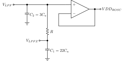
Figure 16: The loop filter SUN_PLL_LPF on VLPF, followed by the buffer SUN_PLL_BUF that drives the oscillator supply VDD_ROSC. C1 is 22 unit capacitors, C2 is 3, so the zero sits where the equations above put it
Divider
The divider is modelled as
\[K_{div} = \frac{1}{N}\]
Figure 17: The feedback divider SUN_PLL_DIVN: five flip-flops wired as toggles, each clocking the next, dividing CK by 32 to make CK_FB
Loop transfer function
With the loop transfer function we can start to model what happens in the linear loop. What is the phase response, and what is the gain response.
\[L(s) = \frac{ K_{osc} K_{pd} K_{lp} H_{lp}(s) }{N s}\]Python model
I’ve made a python model of the loop, you can find it at sun_pll_sky130nm/jupyter/pll - interactive
In the jupyter notebook below you can find some more information on the phase/frequency detector, and charge pump.
Below is a plot of the loop gain, and the transfer function from input phase to divider phase.
We can see that the loop gain at low frequency is large, and proportional to $1/s$. As such, the phase of the divided down feedback clock is the same as our reference.
The closed loop transfer function $\phi_{div}/\phi_{in}$ shows us that the divided phase at low frequency is the same as the input phase. Since the phase is the same, and the frequency must be the same, then we know that the output clock will be N times reference frequency.
Which $K_{osc}$ went into that plot matters more than it looks. The schematic simulation gave 1.6 GHz/V; the extracted layout gives 1.01 GHz/V, and the difference is parasitic capacitance in the ring that simply does not exist until the oscillator is laid out. A third of the gain disappears, and since the loop gain is proportional to $K_{osc}$, the crossover moves from 0.59 MHz down to 0.43 MHz and the phase margin from 51 degrees to 43.
Eight degrees is not a catastrophe, and that is rather the point: it is the sort of erosion that is easy to spend twice over without noticing. Extract early, and design the loop with the number the silicon will actually have rather than the one the schematic promised.
It is also worth checking this plot against the assumption we made when we drew the linear model at all. The loop gain crosses 0 dB at 0.43 MHz, and the reference frequency is $256\ \text{MHz}/32 = 8$ MHz, so the loop bandwidth is a nineteenth of the reference. That clears the “one tenth of the reference” rule, which means the model is entitled to be believed. If it had not cleared it, the phase margin the plot reports would be a number about a model that does not describe the circuit — and that is a far worse situation than a poor phase margin, because it looks fine.
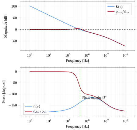
Figure 18: Magnitude and phase of the loop gain and the closed-loop transfer function from input phase to divider phase, using the oscillator gain measured on the extracted layout. The loop crosses 0 dB at 0.43 MHz with 43 degrees of phase margin
The top testbench for the PLL is tran.spi.
I power up the PLL and wait for the output clock to settle. The frequency is measured the way a counter would measure it: find every rising edge of CK and take the reciprocal of the interval between consecutive edges. See freq.py.
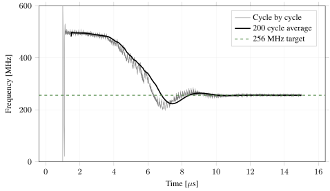
Figure 19: Simulated PLL output frequency from power-up, on the extracted layout at the typical corner. The grey trace is the frequency of each individual cycle and the black one a 200 cycle average; the loop overshoots to about 500 MHz, undershoots past the target, and settles at 256.1 MHz around 12 microseconds
Three things in that plot are worth pausing on.
The loop starts at the top of the oscillator’s range and has to be dragged down, so the first microsecond is not feedback at all, it is the control node charging. Then the loop takes over, overshoots past the target, and rings once before settling. That single undershoot is the second order response the phase margin describes; 43 degrees is what one visible ring looks like.
The grey band does not narrow as the loop settles. That is not the simulation failing to converge, and it is not an error the loop could correct: the charge pump delivers its correction as a pulse once per reference period, so the oscillator is kicked 8 million times a second whatever the loop is doing. In a real chip this is the reference spur, and it is the reason a PLL’s output is never as clean as its reference.
Settling takes about 12 microseconds here, against roughly 8 in earlier versions of this design. The loop got slower because the oscillator got slower: the extracted layout has a third less gain than the schematic, and loop bandwidth is proportional to that gain. Nothing was designed differently; the parasitics simply arrived.
You can find the schematics, layout, testbenches, python script etc at SUN_PLL_SKY130NM
Below are a couple layout images of the finished PLL
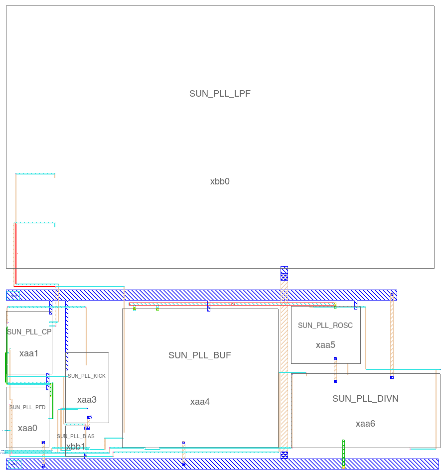
Figure 20: Floorplan of the SUN_PLL layout; the loop filter capacitor SUN_PLL_LPF dominates the area above the PLL blocks
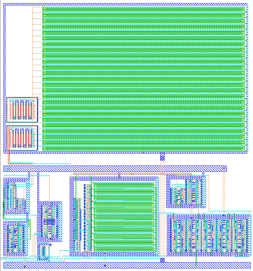
Figure 21: Finished SUN_PLL layout showing the loop filter capacitor array and the PLL blocks along the bottom
Summary
The one-page version of this chapter:
- Everything on the chip wants a clock, and every clock is a compromise between frequency accuracy (ppm), phase noise and power
- A crystal gives the accurate reference; the PLL multiplies it up to the frequency the system needs
- PFD turns phase error into pulse width, the charge pump into charge, the loop filter into a control voltage, the oscillator into frequency, and the divider closes the loop
- The type-II loop needs its zero: C1 sets the zero with R, C2 cleans the ripple, and the loop bandwidth balances reference noise against VCO noise
- Inside the bandwidth the PLL follows the reference; outside, the oscillator is on its own - phase noise plots read exactly that way
- SUN_PLL is the whole story in five schematics: ROSC, PFD, charge pump, loop filter, divider
Would you like to know more?
Back in 2020 there was a Master student at NTNU on PLL. I would recommend looking at that thesis to learn more, and to get inspired Ultra Low Power Frequency Synthesizer.
A Low Noise Sub-Sampling PLL in Which Divider Noise is Eliminated and PD/CP Noise is Not Multiplied by N2 1
All-digital PLL and transmitter for mobile phones 2
A 2.9–4.0-GHz Fractional-N Digital PLL With Bang-Bang Phase Detector and 560-fsrms Integrated Jitter at 4.5-mW Power 3
-
X. Gao and E. A. M. Klumperink and M. Bohsali and B. Nauta, A Low Noise Sub-Sampling PLL in Which Divider Noise is Eliminated and PD/CP Noise is Not Multiplied by $N ^2$ 2009 https://doi.org/10.1109/JSSC.2009.2032723 ↩
-
R. Staszewski and J. Wallberg and S. Rezeq and C.-M. Hung and O. Eliezer and S. Vemulapalli and C. Fernando and K. Maggio and R. Staszewski and N. Barton and M.-C. Lee and P. Cruise and M. Entezari and K. Muhammad and D. Leipold, All-digital PLL and transmitter for mobile phones 2005 https://doi.org/10.1109/JSSC.2005.857417 ↩
-
D. Tasca and M. Zanuso and G. Marzin and S. Levantino and C. Samori and A. L. Lacaita, A 2.9–4.0-GHz Fractional-N Digital PLL With Bang-Bang Phase Detector and 560-$\mathrmfs\mathrmrms$ Integrated Jitter at 4.5-mW Power_ 2011 https://doi.org/10.1109/JSSC.2011.2162917 ↩