TFE4188 - Lecture 8

Clocks and PLLs

1

Goal

Why do we need to generate clocks

Introduction to PLLs

2

Why

3

Digital

Radio

Energy harvesters

Switched regulators

ADCs

Accurate delay

SC filters

...

4
5
6
7

PLL

8
9
10
11
12

\[A_m(t) \times cos\left( 2 \pi f_{carrier}t + \phi_{m}(t)\right)\]

13
14
15

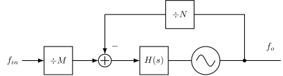
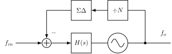
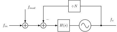
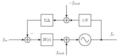
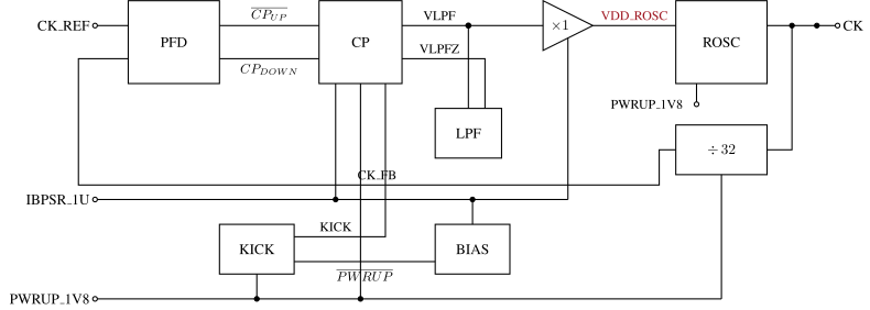
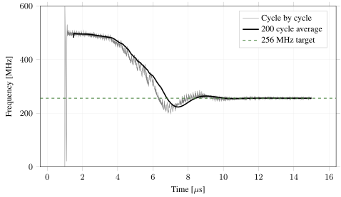
PLL Example

16
17

PLLs need calculation!

#noCowboyDesign

18

\[\phi(t) = 2 \pi \int_0^t f(\tau) d\tau\]

19

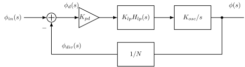
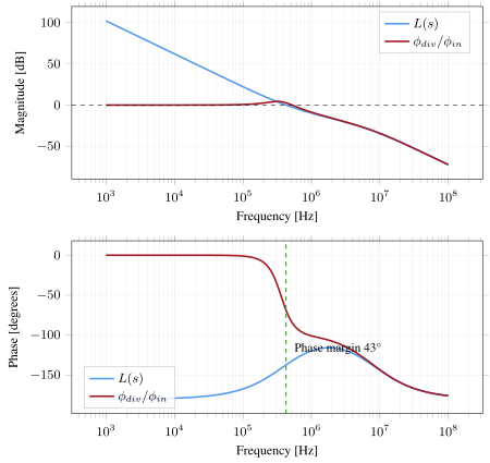
Loop gain

\(\frac{\phi_d}{\phi_{in}} = \frac{1}{1 + L(s)}\)

\[L(s) = \frac{ K_{osc} K_{pd} K_{lp} H_{lp}(s) }{N s}\]

20

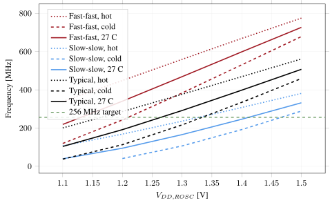
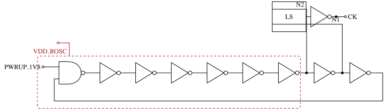
Controlled oscillator

\[K_{osc} = 2 \pi\frac{ df}{dV_{cntl}}\]
21
22

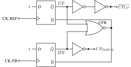
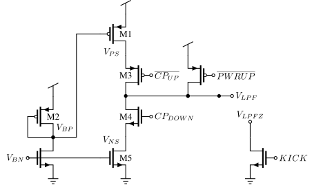
Phase detector and charge pump

\[K_{pd} = \frac{I_{cp}}{2 \pi}\]

23

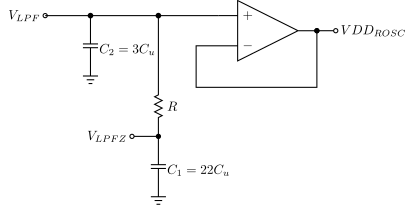
Loop filter

\[K_{lp}H_{lp}(s)= K_{lp}\left(\frac{1}{s} + \frac{1}{\omega_z}\right)\]

\[K_{lp}H_{lp}(s) = \frac{1}{s(C_1 + C_2)}\frac{1 + s R C_1}{1 + sR\frac{C_1C_2}{C_1 + C_2}}\]
24

Divider

\[K_{div} = \frac{1}{N}\]

25

Loop transfer function

\[L(s) = \frac{ K_{osc} K_{pd} K_{lp} H_{lp}(s) }{N s}\]

26
27
28
29

Summary

  • Everything on the chip wants a clock, and every clock is a compromise between frequency accuracy (ppm), phase noise and power
  • A crystal gives the accurate reference; the PLL multiplies it up to the frequency the system needs
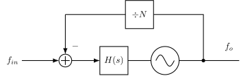
  • PFD turns phase error into pulse width, the charge pump into charge, the loop filter into a control voltage, the oscillator into frequency, and the divider closes the loop
  • The type-II loop needs its zero: C1 sets the zero with R, C2 cleans the ripple, and the loop bandwidth balances reference noise against VCO noise
  • Inside the bandwidth the PLL follows the reference; outside, the oscillator is on its own - phase noise plots read exactly that way
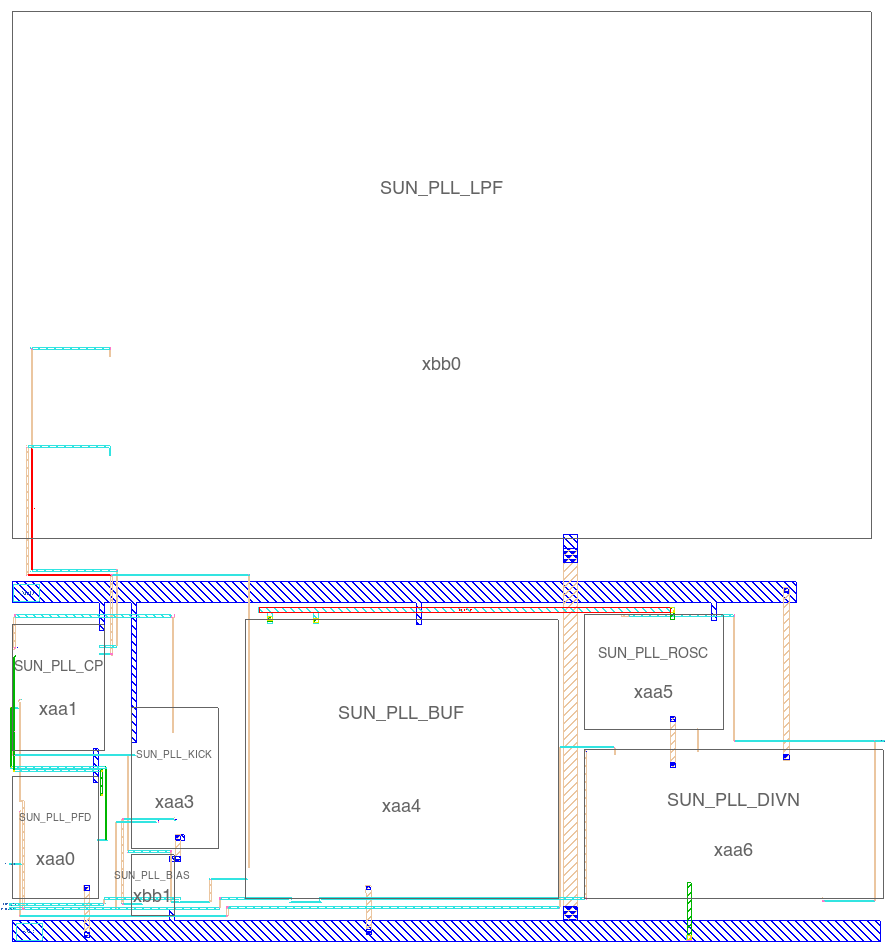
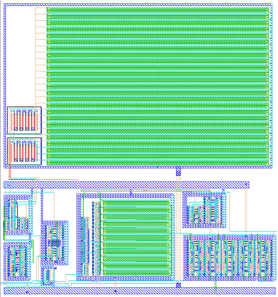
  • SUN_PLL is the whole story in five schematics: ROSC, PFD, charge pump, loop filter, divider
30

Would you like to know more?

31
32

Thanks!

33