Table of contents
- Routing
- Bandgap voltage reference
- A voltage complementary to temperature (CTAT)
- A current proportional to temperature (PTAT)
- How to combine a CTAT with a PTAT ?
- Widlar reference
- Brokaw reference
- Low voltage bandgap
- Curvature correction
- MOS references
- The native threshold is set when the ingot is grown
- FD-SOI moves the problem, it does not remove it
- The back gate is a trimming knob, not a reference
- Bias
- Summary
- Would you like to know more?
Keywords: VREF, IREF, VD, BGAP, LVBGAP, VI, GMCELL
In our SPICE testbenches, and trial schematics, it’s common to include voltage sources and current sources, like the symbols in Figure 1.
The ideal voltage source, or ideal current source, does not exist in the real world. There is no such thing.
We can come close to creating a voltage source, a known voltage, with a low source impedance, but not zero impedance. And it won’t be infinitely fast either. If we suddenly decide to pull 1 kA from a lab supply I promise you the voltage will drop.
How do we create something that is a good enough voltage and current source on an IC? That’s the goal of this chapter. To give you an introduction to “voltage sources” and “current sources” that we can make on an integrated circuit.
But before we take a look at the voltage and current source, I want you to think about how you would route a current, or a voltage on an IC.
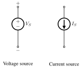
Figure 1: Symbols for voltage source and current source
Routing
Assume we have a known voltage on our IC, a reference voltage. How can we make sure we can share that voltage across an IC?
A voltage is only defined between two points. There is no such thing as the voltage at a point on a wire, nor voltage in a node. Yes, I know we say that, but it’s not right. What we forget is that by voltage in a node we always, always mean voltage in a node referred to ground.
We’ve invented this magical place called ground, the final resting place of electrons, and we have agreed that voltages refer to that point.
As such, when we say “Voltage in node A is 1V”, what we actually mean is “Voltage in node A is 1 V referred to ground”.
Maybe you now understand why we can’t just route a voltage across the IC, the other side might not have the same ground. The other side might have a different impedance to ground, and the impedance might be a function of time, voltage, frequency temperature, pressure and presence of gremlins.
Consider Figure 2. The ground impedance may depend on time, voltage, frequency, temperature, pressure (yes, stress in silicon can change the band structure, thus the conduction band energy levels, and thus the available charge carriers in the conduction band).
If there is no current flowing in the ground impedance at the destination we may be OK, but usually, there is some current flowing into ground at the destination. There is a circuit there.
If we choose to route a reference as a voltage we need to be careful with the ground.
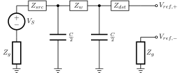
Figure 2: Voltage source with ground impedance. Routing long distances it’s not possible to guarantee we have the same ground impedance at the destination.
Most of the time, in order not to think about the ground impedance, we choose to route a known quantity, the reference, as a current instead of a voltage. That means, however, we must convert from a voltage to a current, but we can do that with a resistor (you’ll see later), and as long as the resistor is the same on the other side of the IC, then we’ll know what the voltage is.
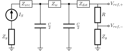
Figure 3: Routing a reference as a current.
Resistors have finite matching across die, let’s say 2 % 3-sigma variation. A limitation on how accurate we can distribute reference across the IC with current method.
For most voltage regulators (think about the circuit that delivers the digital voltage for an MCU) 2 % may be an acceptable portion of the error budget. For a battery charger, however, the termination voltage of Li-ion batteries need to be precise, more accurate than 1 %.
For that application we cannot distribute current, we must distribute voltage, but we need to care deeply about ground.
But how can “It’s better to distribute a voltage as a current across the IC, it’s more accurate” and “If you need something really accurate, you must distribute voltage” both be true?
Imagine I have a 0.5 % 3-sigma accurate voltage reference at 1.22 V, that’s a sigma of 2 mV. I need this reference voltage on a block on the other side of the IC, I don’t want to distribute voltage, because I don’t know that the ground is the same on the other side, at least not to a precision of 2 mV. I convert the voltage into a current, however, I know the R has a 2 % 3-sigma across die, so my error budget immediately increases to 2.06%.
But what if I must have 0.5 % 3-sigma voltage in the block? For example in a battery charger, where the 4.3 V termination voltage must be 1 % accurate? I have no choice but to go with voltage directly from the reference, but the key point, is then the receiving block cannot be on the other side of the IC. The reference must be right next to my block.
I could use two references on my IC, one for the ADC and one for the battery charger. Ask yourself, “Why do we care if there are two references?” And the answer is “Silicon area is expensive, to make things cheap, we must make things small”,
in other words, we should not duplicate features unless we absolutely have to.
Bandgap voltage reference
One of the ways to create a known reference on an integrated circuit is the “bandgap voltage reference”. There are flavors of bandgaps, but all rely on the bandgap of silicon, which is about 1.12 eV.
We can’t access the bandgap voltage directly, but we can use the fact that diodes, and BJTs all have a voltage across the PN junction of about 1.12 V at absolute zero (actually, slightly higher, maybe 1.2 V), and that they have a well known temperature dependence from that point.
A voltage complementary to temperature (CTAT)
A diode connected bipolar transistor, shown in Figure 4, or indeed a PN diode, assuming a fixed current, will have a voltage across that is temperature dependent
\[I_D = I_S \left(e^{\frac{V_{BE}}{V_T}} - 1\right) + I_B \approx I_S e^{\frac{ V_{BE}}{V_T}}\]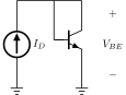
Figure 4: Diode connected bipolar transistor
As $I_S$ is much smaller than $I_C$ we can ignore the -1, and we assume that the base current is much smaller than the collector current.
Re-arranging for $V_{BE}$ and inserting for
\[V_T = \frac{kT}{q}\] \[V_{BE} = \frac{k T}{q} \ln{\frac{I_C}{I_S}}\] \[I_S = q A n_i^2 \left[\frac{D_n}{L_n N_A} + \frac{D_p}{L_p N_D}\right]\]From this equation, it looks like the voltage $V_{BE}$ is proportional to temperature, however, it turns out that the $V_{BE}$ decreases with temperature due to the temperature dependence of $I_S$.
The $V_{BE}$ is almost linear with temperature with a property that if you extrapolate the $V_{BE}$ line to zero Kelvin, then all diode voltages seem to meet at one voltage, $V_{G0} \approx 1.2$ V. That number is close to, but not the same as, the silicon bandgap you look up in a table: the gap is 1.12 eV at room temperature and 1.17 eV at zero Kelvin, while the intercept these lines extrapolate to is around 1.20 to 1.22 V, because the extrapolation also drags the temperature dependence of $I_S$ along with it. It is a voltage, not an energy, and the reference is named after it.
To see the temperature coefficient, I find it easier to re-arrange the equation above.
Some algebra (see Diodes)
\[V_{BE} = \frac{kT}{q}(\ell - 3 \ln T) + V_G\]The $\ell$ is a temperature independent constant given by
\[\begin{split} \ell= \ln{I_C} - \ln{qA} - \ln{\left[\frac{D_n}{L_n N_A} + \frac{D_p}{L_p N_D}\right]} \\ - 2 \ln{2} - \frac{3}{2} \ln{m_n^*} - \frac{3}{2}\ln{m_p^*} - 3 \ln{\frac{2 \pi k}{h^2}} \end{split}\]And if we plot the diode voltage, we can see that the voltage decreases as a function of temperature.
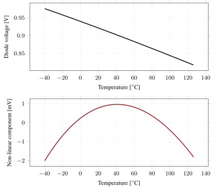
Figure 5: Diode voltage versus temperature. Bottom plot shows deviation from a straight line.
A current proportional to temperature (PTAT)
If we take two diodes, or bipolars, biased at different current densities, as shown in Figure 6, then
\[V_{D1} = V_T \ln{\frac{I_{D}}{I_{S1}}}\] \[V_{D2} = V_T \ln{\frac{I_{D}}{I_{S2}}}\]The OTA will force the voltage on top of the resistor to be equal to $V_{D1}$, thus the voltage across the resistor $R_1$ is
\[V_{D1} - V_{D2} = V_T \ln{\frac{I_{D}}{I_{S1}}} - V_T \ln{\frac{I_{D}}{I_{S2}}} = V_T \ln{\frac{I_{S2}}{I_{S1}} } = V_T \ln N\]This is a remarkable result. The difference between two voltages is only defined by Boltzmann’s constant, temperature, charge, and a known size difference.
This differential voltage can be used to read out directly the temperature on an IC, provided we can compare to a known voltage.
We often call this voltage $\Delta V_D$ or $\Delta V_{BE}$, and we can see it’s proportional to absolute temperature.
We know that the $V_D$ decreases linearly with temperature, so if we combined a multiple of the $\Delta V_{BE}$ with a $V_D$ voltage, then we should get a constant voltage.
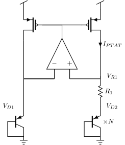
Figure 6: Circuit to create a PTAT current controlled by the resistor and $\Delta V_{BE}$
How to combine a CTAT with a PTAT ?
One method is Figure 7. The voltage across resistor $R_2$ would compensate for the decrease in $V_{D3}$, as such, $R_2$ would be bigger than $R_1$.
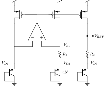
Figure 7: A bandgap voltage reference with a constant output voltage.
Another method would be to stack the $R_2$ on top of $R_1$ as shown in Figure 8.
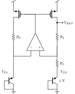
Figure 8: Another bandgap voltage reference with a constant output voltage.
Widlar reference
The first bandgap reference was not Brokaw’s. Bob Widlar built one in 1971 for the LM113, three years before the Brokaw cell that follows, and it is worth starting here. Partly for the history, and partly because it does the entire job with three transistors, three resistors, and no amplifier anywhere. It was published in New developments in IC voltage regulators 1.
Figure 9 is the circuit. It is a two terminal shunt reference: you feed it a bias current down from the supply and it holds its own terminal at $V_{REF}$, the way a zener does, except that it does it at 1.2 V, where no zener will.
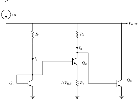
Figure 9: Widlar’s bandgap reference, the first one, from 1971
$Q_1$ is diode connected, so its collector sits one $V_{BE}$ above ground. $Q_3$ holds its own base, which is the collector of $Q_2$, one $V_{BE}$ above ground as well. Both $R_1$ and $R_2$ therefore have very nearly the same voltage across them, and the current ratio falls out of the resistors alone.
\[\frac{I_1}{I_2} = \frac{R_2}{R_1}\]$Q_1$ and $Q_2$ are the same size and share a base, so that difference in current density lands across $R_3$
\[I_2 R_3 = V_{BE1} - V_{BE2} = \frac{kT}{q}\ln{\frac{I_1}{I_2}} = \frac{kT}{q}\ln{\frac{R_2}{R_1}}\]which is PTAT, and depends only on a resistor ratio, so it is as accurate as your matching. That current runs up through $R_2$, and the output is that drop stacked on top of the $V_{BE}$ of $Q_3$.
\[V_{REF} = V_{BE3} + \frac{R_2}{R_3}\frac{kT}{q}\ln{\frac{R_2}{R_1}}\]CTAT plus PTAT, and we are about to do it again with an amplifier. With $R_2/R_1 = 10$ the log term is about 60 mV at room temperature, $R_2/R_3 = 10$ scales that to 600 mV, and stacked on a 600 mV $V_{BE}$ you land at the 1.2 V the LM113 was sold as.
Notice what is doing the job of the OTA. $Q_3$ is the gain element. If the terminal tries to rise, the collector of $Q_2$ follows it up, $Q_3$ conducts harder, and shunts the extra current away. The loop closes through a single transistor. That is why the circuit fits in a process where you count your transistors, and it is also why it has less loop gain, and therefore worse line regulation, than the amplifier based cells that came after it. Widlar was not short of ideas, he was short of devices.
One more thing worth taking from this circuit is where the current density ratio comes from. Here it is $R_2/R_1$, a ratio of resistors. In the Brokaw cell it is an emitter area ratio instead. Both work, and both are asking a ratio of like things to be accurate, which is the only kind of accuracy an integrated circuit actually has.
Brokaw reference
Paul Brokaw was a pioneer within reference circuits ( I met him once in the restroom queue in Tropisueno behind the Marriot hotel in SF during ISSCC). Below is the Brokaw reference, which I think was first published in A simple three-terminal IC bandgap reference 2.
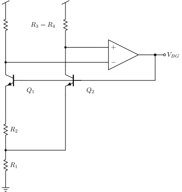
Figure 10: Brokaw bandgap voltage reference
The opamp ensures the two bipolars have the same current. $Q_1$ is larger than $Q_2$. The $\Delta V_{BE}$ is across the $R_2$, so we know the current $I$. We know that $R_1$ must then have $2I$.
The voltage at the output will then be.
\[V_{BG} = V_{G0} + (m-1)\frac{kT}{q}\ln{\frac{T_0}{T}} +T\left[\frac{k}{q}\ln{\frac{J_2}{J_1}}\frac{2R_1}{R_2} - \frac{V_{G0}- V_{be0}}{T_0}\right]\]where $V_{G0}$ is the bandgap extrapolated to zero Kelvin, $V_{be0}$ is the base emitter voltage measured at a temperature $T_0$, the $J$’s are the current densities, and $m$ is the exponent that collects the temperature dependence of the saturation current and of the bias current - about 3 for a diode run at constant current, and we will come back to it in the curvature section.
Read the three terms. The first is a constant. The third is proportional to $T$, and the resistor ratio is the knob on it. The second is the awkward one: it is proportional to $T\ln{T}$, and no resistor ratio can touch it.
Now, what does “constant output” mean? The tempting answer is to make the bracket zero, which kills the term in bare $T$ and leaves
\[V_{BG} = V_{G0} + (m-1)\frac{kT}{q}\ln{\frac{T_0}{T}}\]That is not flat. Differentiate it: at $T = T_0$ the slope is $-(m-1)k/q \approx -170$ uV/K, or about $-140$ ppm/K, which is a hundred times worse than the reference you were trying to build. The $T\ln{T}$ term has a slope of its own, and setting the bracket to zero leaves it uncancelled.
What we actually want is zero slope at the temperature we care about. Take the derivative of the whole expression, set it to zero at $T_0$, and the condition is that the bracket must equal $(m-1)k/q$ rather than zero:
\[\frac{k}{q}\ln{\frac{J_2}{J_1}}\frac{2R_1}{R_2} = \frac{V_{G0}-V_{be0}}{T_0} + (m-1)\frac{k}{q}\]so the resistor ratio is
\[\frac{R_1}{R_2} = \frac{V_{G0} - V_{be0} + (m-1)\frac{kT_0}{q}}{2 T_0 \frac{k}{q}\ln(\frac{J_2}{J_1})}\]and the output voltage at that point is not the bandgap, but a little above it
\[V_{BG}(T_0) = V_{G0} + (m-1)\frac{kT_0}{q} \approx 1.25 \text{ V}\]This is worth remembering, because it surprises people: a bandgap reference trimmed for zero temperature coefficient sits around 1.25 V, not at the 1.20 V bandgap it is named after. The extra 50 mV is exactly the price of cancelling the slope of the $T\ln{T}$ term at one temperature.
In typical simulations, the variation can be
low over the temperature range. The second order error is the remaining error from
With the resistor ratio picked so that the slope vanishes at $T_0$, the bracket is $(m-1)k/q$, so the term in bare $T$ becomes $(m-1)\frac{k}{q}T$ and what remains is
\[V_{BG} = V_{G0} + (m-1)\frac{kT}{q}\ln{\frac{T_0}{T}} + (m-1)\frac{k}{q}T\] \[V_{BG} = V_{G0} + (m-1)\frac{kT}{q}\left[1 + \ln{\frac{T_0}{T}}\right]\]a curve with zero slope at $T_0$ and a maximum there. Everywhere else it falls away, and that bow is the second order error we are left with.
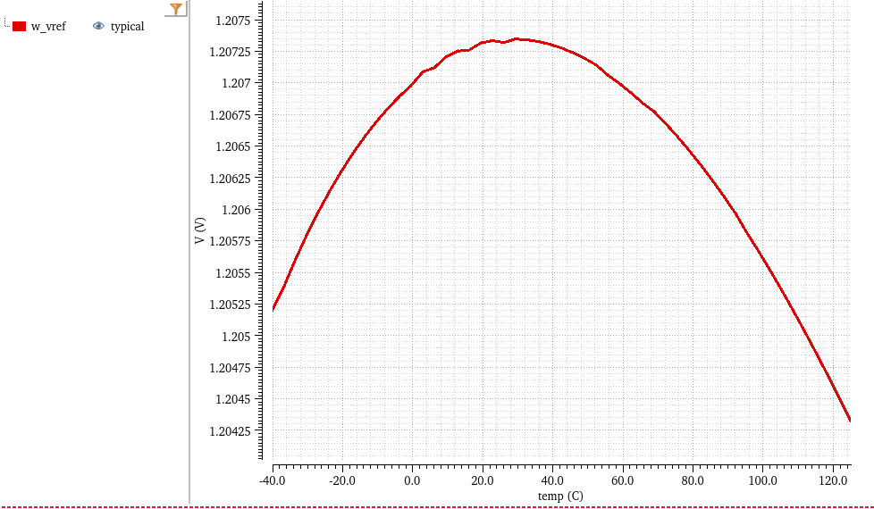
Figure 11: Simulation of a Brokaw reference in GF 130 nm
Read the axes before anything else. The whole vertical range is about 3 mV on an output of 1.207 V, so the curve you are looking at is flat to roughly 15 ppm/K over the range - the plot is magnified enormously.
Then look at the shape. It rises, peaks a little above room temperature, and falls away on both sides. That peak is not an accident: it is the temperature where we chose the slope to be zero, and the resistor ratio put it there. The bow either side of it is exactly the $T\left[1 + \ln{(T_0/T)}\right]$ term we could not cancel with a resistor ratio, and the curvature section later in this chapter is about getting rid of it.
Over corners, I do expect that there is variation, as we can see from Figure 12.
Two things move, and they are worth separating. The first is a vertical offset of roughly $\pm 10$ mV, about $\pm 0.8$ %: that is the absolute accuracy of the reference, and it comes from resistor and $V_{BE}$ spread. The second is more interesting: the peak moves. The slow corner is still climbing at 125 C while the fast corner has already turned over near 0 C.
A moving peak means the linear balance has shifted, not that the curvature term misbehaved. The bracket we so carefully set to $(m-1)k/q$ is only zero at typical: when the resistors and $V_{BE}$ walk to a corner, the bracket picks up a residue, and a residue in the bracket is a term proportional to $T$, which tilts the whole curve and drags the maximum with it.
We could include trimming of PTAT to calibrate for the remaining error, however, if we wanted to remove the linear gradient, we would need a two point temperature test of every IC, which is too expensive for low-cost devices.
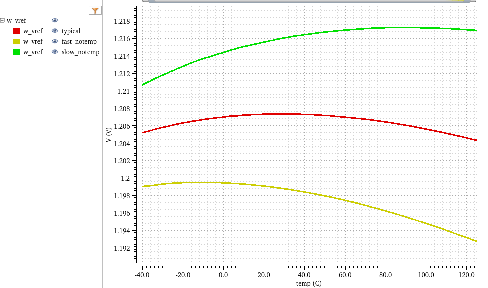
Figure 12: Typical, slow and fast corner simulation of the Brokaw bandgap. The legend’s “notemp” corners hold temperature-dependent model parameters at their typical values, so the spread shown is process alone
Low voltage bandgap
The Brokaw reference, and others, have a 1.2 V output voltage, which is hard to make if your supply is below about 1.4 V. As such, people have investigated lower voltage references. The original circuit was presented by Banba A CMOS bandgap reference circuit with sub-1-V operation 3
In real ICs though, you should ask yourself long and hard whether you really need these low-voltage references. Most ICs today still have a high voltage, either 1.8 V or 3.0 V.
If you do need them, consider the circuit in Figure 13. We have two diodes at different current densities. The $\Delta V_D$ will be across $R_1$. The voltage at the input of the OTA will be $V_D$ and the OTA will ensure the both inputs are equal.
The current will then be
\[I_1 = \frac{\Delta V_{D}}{R_1}\]and we know the current increases with temperature, since $\Delta V_D$ increases with temperature.
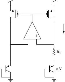
Figure 13: PTAT current generator
I use $\Delta V_{BE}$ and $\Delta V_D$ interchangeably, apologies.
In Figure 14 we copy the $V_D$ to another node, and place it across a second resistor $R_2$.
The current in this second resistor is then
\[I_2 = \frac{V_D}{R_2}\]and we know the current decreases with temperature, since $V_D$ decreases with temperature.
From before, we know the current in $R_1$ is proportional to temperature. As such, if we combine the two current with the correct proportions, then we can get a current that does not change with temperature.
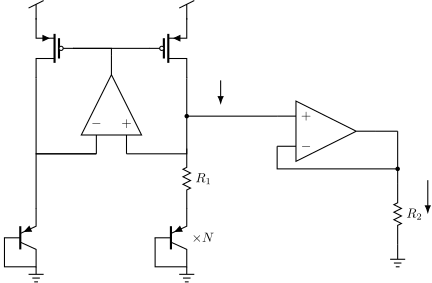
Figure 14: Extending the PTAT current generator
Let’s remove the OTA, and connect $R_2$ directly to $V_D$ nodes, as shown in Figure 15.
You should convince yourself of the fact that this does not change $I_1$.
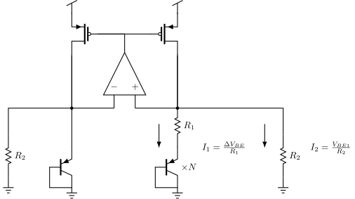
Figure 15: The Banba bandgap voltage reference core
It does, however, change the current in the PMOS. Provided we scale $R_2$ correctly, then the PTAT $I_1$ can compensate for CTAT $I_2$, and we have a current that is independent of temperature.
\[I_{PMOS} = \frac{V_D}{R_2} + \frac{\Delta V_D}{R_1}\]Assuming we copy the current into another resistor $R_3$, as shown in Figure 16, we can get a voltage that is
\[V_{OUT} = R_3\left[\frac{V_D}{R_2} + \frac{\Delta V_D}{R_1}\right]\]We can choose the output voltage freely, and it can be lower than 1.2 V.
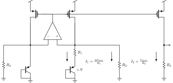
Figure 16: The Banba bandgap voltage reference
Curvature correction
Go back and look at Figure 12 again. Over corners the reference is not flat, and even the typical curve in Figure 11 has a bend in it. That bend is not noise, and it is not a mistake in the design. It is a term we agreed to ignore, and it is time to stop ignoring it.
We picked the resistor ratio so the slope vanishes at one temperature. That flattens the curve where we chose to flatten it, and it does nothing at all to the shape of what is left,
\[V_{BG} = V_{G0} + (m-1)\frac{kT}{q}\left[1 + \ln{\frac{T_0}{T}}\right]\]and that is the bow you can see in Figure 11. It comes from the temperature dependence of $I_S$ - the $-3\ln{T}$ we carried through the $V_{BE}$ algebra earlier - together with the temperature dependence of the bias current itself. That is where the $-1$ comes from: if the diode current is PTAT, as it is in every circuit in this chapter, it contributes one power of $T$ and the coefficient becomes $m-1$ rather than $m$. With $m \approx 3$ the coefficient is about 2. Be careful with that number: the $3$ assumes temperature independent diffusion, and measured devices sit nearer 3.6 to 4, so a design that trims $R_4$ from theory alone will be off.
No choice of $R_1/R_2$ can remove it. A resistor ratio can only add something proportional to $T$, and what is left over is proportional to $T\ln{T}$. If we want to cancel it, we have to build a $T\ln{T}$ term.
Here is where one comes from. Take two identical bipolars at the same temperature. The difference of their base-emitter voltages is
\[V_{BE,A} - V_{BE,B} = \frac{kT}{q}\ln{\frac{I_A}{I_B}}\]and this one is exact, not an approximation. $I_S$ cancels completely, because it is the same device at the same temperature.
This is the same $\Delta V_{BE}$ we have used all chapter, and every time so far the current ratio has been a fixed number set by device sizes. That is what made it PTAT. So make the ratio depend on temperature instead: bias $Q_A$ with a PTAT current, and $Q_B$ with the temperature compensated current the reference already produces. Then $I_A/I_B = K T/T_0$ and
\[V_{BE,A} - V_{BE,B} = \frac{kT}{q}\ln{K} + \frac{kT}{q}\ln{\frac{T}{T_0}}\]The first term is PTAT, and we know what to do with those. The second term is the $T\ln{T}$ we needed, and it comes with the right sign.
Figure 17 turns that voltage into a current. The OTA holds the right hand end of $R_4$ at $V_{BE,A}$, the left hand end sits on $V_{BE,B}$, and $M_{PC}$ supplies whatever current that requires. $M_{PD}$ copies it into the summing node from Figure 16, so the $V_{OUT}$ of that circuit becomes
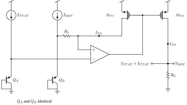
Figure 17: Curvature correction. $Q_A$ and $Q_B$ are the same device at different bias currents, so the voltage across $R_4$ carries a $T\ln{T}$ term.
\[I_{NL} = \frac{V_{BE,A} - V_{BE,B}}{R_4} = \frac{kT}{qR_4}\left[\ln{K} + \ln{\frac{T}{T_0}}\right]\] \[V_{REF} = R_3\left[\frac{V_D}{R_2} + \frac{\Delta V_D}{R_1} + I_{NL}\right]\]The curvature the $V_D$ term brings in is $\frac{R_3}{R_2}(m-1)\frac{kT}{q}\ln{\frac{T_0}{T}}$, the curvature the new branch adds is $\frac{R_3}{R_4}\frac{kT}{q}\ln{\frac{T}{T_0}}$, and they cancel when
\[R_4 = \frac{R_2}{m-1}\]for which $R_2$ and $R_4$ must be the same kind of resistor: the ratio only holds over temperature if their temperature coefficients cancel.
which is a nice result. The correction is set by a resistor ratio, like everything else in this chapter, and with $m \approx 3$ it makes $R_4$ about half of $R_2$. The $\frac{kT}{q}\ln{K}$ half of $I_{NL}$ is PTAT, so it simply adds to the PTAT current already there, and you retrim $R_1$ to take it back out.
Three things to watch.
$I_{NL}$ leaves $R_4$ and flows into the emitter of $Q_B$, so $Q_B$ does not carry exactly $I_{REF}$. It is a small perturbation, but it is real, and it makes the sizing slightly iterative.
$V_{BE,A}$ has to stay above $V_{BE,B}$ across the whole temperature range, or the current in $R_4$ reverses and the loop runs out of room. The ratio is $K T/T_0$, so pick $K$ large enough that it is still comfortably above one at the cold end.
And $m$ is not a number the foundry hands you to three digits. Curvature correction typically buys a factor of five to ten in temperature drift, not a factor of a thousand, and what it buys is limited by how well you know $m$. It is worth the area when you need 10 ppm/$^\circ$C. It is a waste of area when 50 ppm/$^\circ$C is fine, which it usually is.
MOS references
Recognise this one. Do not build it.
Everything so far has needed a bipolar. In a pure CMOS process that is irritating, and the temptation is obvious. The MOS transistor has a threshold voltage, thresholds fall with temperature at roughly $-1$ mV/K, and if two devices have different thresholds then the difference between them ought to be flat. A reference with no bipolar in it.
If you read older books you will find this done with an enhancement device and a depletion device. Forget that circuit. It relied on a threshold below zero, so that a device with its gate tied to its own source still conducted, and in a nanoscale CMOS process there is no such device. Essentially everything on the menu sits at 300 mV or more. What you get instead is a handful of implant flavours, standard, low $V_t$ and high $V_t$, separated by a hundred millivolts or so, plus the native device, which skips the channel implant altogether and is the only one that lands anywhere near zero.
So the modern version of the idea pairs two of those flavours, and it looks like Figure 18.
You have seen this loop before, or rather you are about to see it: it is the GM cell from later in this chapter, with the size ratio taken out and a second implant put in its place. The PMOS mirror forces the same current down both branches, $M_1$ and $M_2$ have the same $W/L$, and the only thing left that distinguishes them is which channel implant they were given.
Both gates sit on the same node, so $V_{GS1} = V_{GS2} + I R$, and writing each gate-source voltage as a threshold plus an overdrive
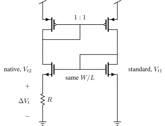
Figure 18: A reference built on the difference between two threshold voltages. Learn to recognise it. Do not build it.
\[I R = (V_{t1} + V_{eff1}) - (V_{t2} + V_{eff2})\]Equal current in equal $W/L$ means equal overdrive, so the $V_{eff}$ terms cancel and what is left is the entire reference
\[I = \frac{V_{t1} - V_{t2}}{R} = \frac{\Delta V_t}{R}\]MOS based references that rely on the difference between two threshold voltages are very risky and should not be attempted.
I want you to leave this section able to recognise that circuit, and unwilling to build it. Process control over the two threshold sources is poor, and their stability is poor, so the difference is neither well controlled nor stable.
Put Figure 18 next to Figure 20 and the problem is visible in one look. They are the same loop. The GM cell puts a 4:1 size ratio in it, and a size ratio is lithography, two drawings of the same thing, which is about as well controlled as anything on a die gets. This circuit puts the difference of two channel implants in the same place. Those are two separate recipes, aimed separately, monitored separately, and drifting separately. Nothing makes them move together.
Watch what the numbers do. Take standard against low $V_t$: two devices at maybe 450 mV and 350 mV, each with a spread of $\pm 50$ mV over process. Each threshold on its own is known to about $\pm 12$ %. The difference you actually use is 100 mV, and if the two spreads are independent it is known to about $\pm 70$ %. If they happen to move in opposite directions it is worse than that, and nothing in the process says they will not. Subtracting two similar, poorly known numbers is the worst thing you can do to an error budget.
The native threshold is set when the ingot is grown
Reach for the native device to get a bigger difference and you have picked the least controlled transistor in the process. Its threshold is whatever is left when you leave the channel implant out, which means it rides on the doping of the silicon underneath it, and that is not a number the fab sets.
Think about where it does get set. Not in an implanter, where the dose is metered to about a percent and measured on every lot. It is fixed when the ingot is grown, by how much boron went into the melt before the crystal was pulled out of it, and the boule is usually not even grown by the company that builds your chip. You buy wafers, and what you buy is a resistivity range, not a resistivity.
It is worse than a range. Boron has a segregation coefficient below one, so it would rather stay in the melt than join the crystal. As the boule is pulled the melt gets steadily richer, and the silicon that freezes out near the tail end is more heavily doped than the silicon at the seed end, by tens of percent over the length of one crystal. Wafers sliced from the two ends of the same boule are not the same wafer. There is a radial gradient across each wafer on top of that, and well proximity and STI stress move it again locally.
None of this is visible to the fab’s process control, which watches implants and etches, and none of it is correctable there either. So one end of your subtraction is set by an implanter recipe inside the fab, and the other end is set by a crystal grower at a different company, to a different specification, probably on a different continent. Those two numbers have no reason on earth to move together. In most PDKs the native device duly comes with the widest corners and the thinnest model guarantees of anything on the menu.
If the process runs on epitaxial wafers the native device sees the epi layer rather than the bulk, and epi doping is better controlled than a pulled crystal. It is still a deposition specification rather than a metered implant, and it is still usually somebody else’s specification.
Compare that with what a bandgap does. A bandgap gets its number from $E_g$ of silicon. That is a property of the material, it is the same in every fab on earth, and no process engineer can move it. This circuit gets its number from the difference between an implant recipe and a crystal pull.
Stability is the other half, and trimming does not save you. You can trim out the initial spread in production test, once. Then the thresholds move over the life of the part. NBTI and hot carrier stress shift them, and they shift by different amounts, because the two devices see different fields, different bias and different channel doping. Nothing anchors the difference, so it walks.
The derivation has a hole in it as well. It assumed the two devices are identical apart from $V_t$, which is the only reason the overdrives cancelled. They are not. The implant that moves the threshold also moves the mobility, the body effect coefficient and the subthreshold slope, so $V_{eff1}$ and $V_{eff2}$ do not quite cancel, and what is left over has its own temperature dependence. On top of that $M_2$ has its source $\Delta V_t$ above ground while its bulk is at ground, so the body effect raises $V_{t2}$ by an amount that depends on the answer.
If you need a reference in a pure CMOS process, use the parasitic vertical PNP that every CMOS process has, in the circuits from earlier in this chapter. If what you actually need is a bias current rather than a reference, use the GM cell from later in this chapter. Neither of those asks two implants to agree with each other.
FD-SOI moves the problem, it does not remove it
Everything so far has been a bulk story, and you should ask what happens in a fully depleted process. In FD-SOI the channel is undoped silicon a few nanometres thick sitting on buried oxide, and the threshold is not set by channel doping at all. It is set by the work function of the gate stack, and by the doping of the back plane under the oxide, which is what a regular well and a flip well actually are.
That fixes something real. An undoped channel has no random dopant fluctuation, and random dopant fluctuation is the dominant source of local $V_t$ mismatch in bulk. Two FD-SOI devices side by side match far better than two bulk devices of the same area. If mismatch were the objection, FD-SOI would answer it.
Mismatch was never the objection. The objection is that the two ends of the subtraction are set by unrelated recipes, and in FD-SOI they still are: one by a metal gate work function, the other by an implant under the oxide. Those two have no more reason to track each other than two channel implants did.
The supplier problem does not go away either, it changes address. Fully depleted means the threshold depends on how thick the silicon film is, and that film is a few nanometres of silicon bonded onto oxide by the wafer maker rather than grown by your fab. You have traded a resistivity specification you do not control for a thickness specification you do not control.
The back gate is a trimming knob, not a reference
The back gate is the genuinely interesting part of FD-SOI here. It moves $V_t$ by tens of millivolts per volt, and it moves it electrically, after the wafer is finished. That is a wonderful trimming knob, and it is one of the better reasons to be in FD-SOI at all. It is not a reference, though. Setting a threshold with a voltage means generating that voltage first, and you are back where you started.
One footnote on the advice I just gave, since it was written for bulk. The vertical PNP does not exist in the thin film, so in FD-SOI you cannot simply reach for it. What you do instead is put the bandgap in a hybrid opening, where the film and the buried oxide are removed and you are looking at ordinary bulk silicon again. Every FD-SOI process gives you those, because the I/O and the ESD need them too. The circuit is the same circuit. It just needs somewhere to live.
Bias
Sometimes we just need a current
Voltage to current conversion
With a known voltage, we can convert to a known current with the circuit in Figure 19.
On-chip we don’t have accurate resistors, but for bias currents, it’s usually ok with $\pm 20$ % variation (the variation of R).
Across an IC, we can expect the resistors to match within 2 % percent, as such, we can recreate a voltage with an accuracy of about 2 % difference from the original if we have a second resistor on the other side of the IC.
If we wanted to create an accurate current, then we’d trim the R in production test until the current is what we want.
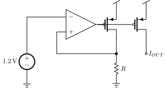
Figure 19: Voltage to current converter
GM Cell
Sometimes we don’t need a full bandgap reference. In those cases, we can use a GM cell, as shown in Figure 20.
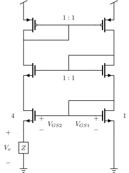
Figure 20: GM cell.
The top PMOS current mirror ensures that both branches have the same current. The middle NMOS current mirror copies the drain voltage on top of the diode connected bottom NMOS to the left NMOS. Consider the bottom transistors, those marked with “1” and “4”. The $V_o$ voltage is
\[V_o = V_{GS1} - V_{GS2} = V_{eff1} + V_{tn} - V_{eff2} - V_{tn} = V_{eff1} - V_{eff2}\]Assuming transistors in strong inversion, then
\[I_{D1} = \frac{1}{2} \mu_n C_{ox} \frac{W_1}{L_1} V_{eff1}^2\] \[I_{D2} = \frac{1}{2} \mu_n C_{ox} 4 \frac{W_1}{L_1} V_{eff2}^2\] \[I_{D1} = I_{D2}\] \[\frac{1}{2} \mu_n C_{ox} \frac{W_1}{L_1} V_{eff1}^2 = \frac{1}{2} \mu_n C_{ox} 4 \frac{W_1}{L_1} V_{eff2}^2\] \[V_{eff1} = 2 V_{eff2}\]Inserted into above
\[V_o = V_{eff1} - \frac{1}{2} V_{eff1} = \frac{1}{2}V_{eff1}\]Still assuming transistors in strong inversion, such that
\[g_{m} = \frac{2 I_d}{V_{eff}}\]we find that
\[I = \frac{ V_{eff1}}{2Z}\]so the impedance sets the transconductance directly
\[g_{m1} = \frac{1}{Z}\]If we use a resistor for $Z$, then the transconductance is set by, and inversely proportional to, that resistor: $g_{m1} = 1/R$. That is the whole point of the circuit, and it is why it is called a constant $g_m$ bias. The transconductance no longer depends on mobility, oxide thickness or threshold voltage - all the things that move with process and temperature - only on a resistor and a device ratio. With a general ratio $K$ between the two devices the result is $g_{m1} = \frac{2}{R}\left(1 - \frac{1}{\sqrt{K}}\right)$, which is $1/R$ at the $K = 4$ drawn here.
We can use other things for $Z$, like a switched capacitor. A capacitor $C_1$ toggled between two nodes at a frequency $f$ moves a charge $C_1 \Delta V$ every cycle, which is an average current $f C_1 \Delta V$, so it behaves as a resistance
\[Z = \frac{1}{f C_1}\]and the transconductance becomes $g_{m1} = f C_1$: set by a clock frequency and a capacitor ratio rather than by a resistor. That is attractive, because a frequency can come from a crystal and a capacitor matches better than a resistor - at the price of the switching noise the switched capacitor chapter worries about.
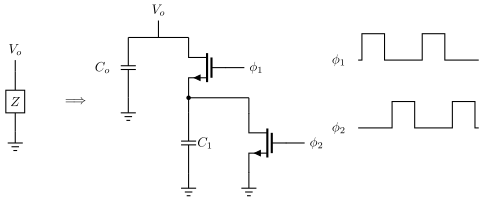
Figure 21: A switched capacitor used as the impedance $Z$, giving $g_{m1} = f C_1$
Every one of these loops can fail to start
There is something missing from every self biased circuit in this chapter, and it is the thing most likely to make your first bias circuit fail in silicon.
Look at the GM cell again, or at any of the OTA based bandgaps. The PMOS mirror says the two branch currents must be equal. The NMOS pair says what that current has to be. Together they have a solution, the one we designed for. But read the statement again: the two branches must agree. Zero current in both branches agrees perfectly well. Every equation in the loop is satisfied, the PMOS rail sits at the supply, the NMOS rail sits at ground, every device is off, and nothing in the circuit has any reason to change.
That is a second, perfectly stable operating point, and a DC simulation is entitled to find either one. Worse, a DC simulation often finds the one you wanted, because the solver started its guess somewhere helpful - and then the chip comes back and the reference never wakes up.
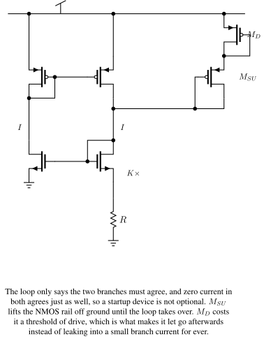
Figure 22: A constant $g_m$ bias with a startup branch. $M_{SU}$ lifts the NMOS rail while it is stuck at ground, and $M_D$ is what makes it let go once the loop is running
The fix is a device that is only on in the dead state, and the first question is which of the two dead rails it should attack. Only one of them can be moved cheaply. The PMOS rail is stuck at $V_{DD}$, and there is nothing useful a device hanging off the supply can do to a node already at the supply. The NMOS rail is stuck at ground, and a PMOS from $V_{DD}$ can lift it. That is the one to go after.
So $M_{SU}$ is a PMOS from the supply onto the NMOS rail, with its gate on that same rail. While the loop is asleep the rail is at ground, $M_{SU}$ has the full supply from gate to source, and it conducts and lifts the rail until the NMOS pair turns on and the loop takes over. As the rail rises, $M_{SU}$’s own drive falls, so it backs off without being told to.
It does not back off far enough, and this is the part that bites in a low-power design. Awake, the NMOS rail only climbs to a gate-source drop, call it 400 mV, which leaves $M_{SU}$ with $\vert V_{GS}\vert = V_{DD} - 400$ mV. In a low-threshold process that is still an on transistor, quietly injecting current into the rail it was supposed to have released. If the loop’s own branch current is a few hundred nanoamps, that injection is not a rounding error — it sets the reference.
$M_D$ is the fix. A second diode-connected PMOS in series means the startup branch needs two thresholds of headroom instead of one, so it stops conducting once the rail has risen. Asleep, the full supply across two diodes is still plenty to get things moving. The cost is a little headroom in a branch that only matters before the reference wakes up, which is the cheapest headroom in the circuit.
Two rules follow from this, and they are worth more than the circuit:
- Always simulate startup as a transient from zero supply, not from a DC operating point. Ramp $V_{DD}$ over a realistic time, and check that the reference comes up every corner, at every temperature, at the slowest supply ramp you can imagine. A bias circuit that only starts in a fast ramp is a bias circuit that will fail on a slow one.
- Check that the startup device really turns off. If it keeps conducting it becomes a leakage path that sets your reference, and the reference is then whatever the startup device felt like, not what the bandgap said.
Summary
The one-page version of this chapter:
- A reference must not move with supply, temperature or process; a bias must track what its circuit needs
- V_BE falls with temperature (CTAT), the difference of two V_BE at a density ratio rises (PTAT, V_T ln N): weight and add for a flat bandgap near 1.2 V
- Widlar and Brokaw are the classic ways to force the PTAT current and do the sum
- Distribute currents, not voltages: a routed V_B collects every IR drop on the die
- The constant-gm loop sets gm = 1/R for everything it biases
- Every self-biased loop is equally happy at zero current - the startup branch is not optional, and it must let go afterwards
Would you like to know more?
New developments in IC voltage regulators 1
A simple three-terminal IC bandgap reference 2
A CMOS bandgap reference circuit with sub-1-V operation 3
A sub-1-V 15-ppm//spl deg/C CMOS bandgap voltage reference without requiring low threshold voltage device 4
The Bandgap Reference 5
The Design of a Low-Voltage Bandgap Reference 6
-
R. Widlar, New developments in IC voltage regulators 1971 https://doi.org/10.1109/JSSC.1971.1050151 ↩ ↩2
-
A. Brokaw, A simple three-terminal IC bandgap reference 1974 https://doi.org/10.1109/JSSC.1974.1050532 ↩ ↩2
-
H. Banba and H. Shiga and A. Umezawa and T. Miyaba and T. Tanzawa and S. Atsumi and K. Sakui, A CMOS bandgap reference circuit with sub-1-V operation 1999 https://doi.org/10.1109/4.760378 ↩ ↩2
-
K. N. Leung and P. Mok, A sub-1-V 15-ppm//spl deg/C CMOS bandgap voltage reference without requiring low threshold voltage device 2002 https://doi.org/10.1109/4.991391 ↩
-
B. Razavi, The Bandgap Reference [A Circuit for All Seasons] 2016 https://doi.org/10.1109/MSSC.2016.2577978 ↩
-
B. Razavi, The Design of a Low-Voltage Bandgap Reference [The Analog Mind] 2021 https://doi.org/10.1109/MSSC.2021.3088963 ↩