Table of contents
Keywords: Range, Antenna Size, Modulation, OFDM, GFSK, pi/4-qpsk, 8-psk, 16 QAM, Bluetooth LE, LP RX, LNA, Mixer, AAF, ADC, BB
Radio’s are all around us. In our phone, on our wrist, in our house, there is Bluetooth, WiFi, Zigbee, LTE, GPS and many more.
A radio is a device that receives and transmits light encoded with information. The frequency of the light depends on the standard. How the information is encoded onto the light depends on the standard.
Assume that we did not know any standards, what would we do if we wanted to make the best radio IC for gaming mice?
There are a few key concepts we would have to know before we decide on a radio type: Data Rate, Carrier Frequency and range, and the power supply.
Data Rate
Data
A mouse reports on the relative X and Y displacement of the mouse as a function of time. A mouse has buttons. There can be many mice in a room, as such, they must have an address , so PCs can tell them apart.
A mouse must be low-power. As such, the radio cannot be on all the time. The radio must start up and be ready to receive quickly.
We don’t know how far away from the PC the mice might be, as such, we don’t know the dB loss in the communication channel. As a result, the radio needs to have a high dynamic range, from weak signals to strong signals. In order for the radio to adjust the gain of the receiver we should include a pre-amble, a known sequence, for example 01010101, such that the radio can adjust the gain, and also, recover the symbol timing.
All in all, the packets we send from the mouse may need to have the following bits.
| What | Bits | Why |
|---|---|---|
| X displacement | 8 | |
| Y displacement | 8 | |
| CRC | 4 | Bit errors |
| Buttons | 16 | One-hot coding. Most mice have buttons |
| Preamble | 8 | Synchronization |
| Address | 32 | Unique identifier |
| Total | 76 |
Rate
Gamers are crazy for speed, they care about milliseconds. So our mice needs to be able to send and receive data quite often.
Assume 1 ms update rate
Data Rate
To compute the data rate, let’s do a back of the envelope estimate of the data, and the rate.
Application Data Rate > 76 bits/ms = 76 kbps

Assume 30 % packet loss

Raw Data Rate > 228 kbps

Multiply by 3.14 > 716 kbps

Round to nearest nice number = 1Mbps
The above statements are a exact copy of what happens in industry when we start design of something. We make an educated guess and multiply by a number. More optimistic people would multiply with $e$.
Carrier Frequency & Range
ISM (industrial, scientific and medical) bands
There are rules and regulations that prevent us from transmitting and receiving at any frequency we want. We need to pick one of the ISM bands, or we need to get a license from governments around the world.
For the ISM bands, there are regions, as seen below.
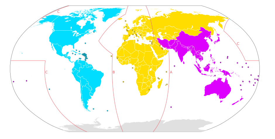
Figure 1: ITU regions that set the ISM band allocations: region 1 (yellow), region 2 (blue), region 3 (pink). Image: Maximilian Doerrbecker (Chumwa), CC BY-SA 2.5, via Wikimedia Commons
- Yellow: Region 1
- Blue: Region 2
- Pink: Region 3
Below is a table of the available frequencies, but how should we pick which one to use? There are at least two criteria that should be investigated. Antenna and Range.
| Flow | Fhigh | Bandwidth | Description |
|---|---|---|---|
| 40.66 MHz | 40.7 MHz | 40 kHz | Worldwide |
| 433.05 MHz | 434.79 MHz | 1.74 MHz | Region 1 |
| 902 MHz | 928 MHz | 26 MHz | Region 2 |
| 2.4 GHz | 2.5 GHz | 100 MHz | Worldwide |
| 5.725 GHz | 5.875 GHz | 150 MHz | Worldwide |
| 24 GHz | 24.25 GHz | 250 MHz | Worldwide |
| 61 GHz | 61.5 GHz | 500 MHz | Subject to local acceptance |
Antenna
For a mouse we want to hold in our hand, there is a size limit to the antenna. There are many types of antenna, but
assume wavelength/4 is an OK antenna size (wavelength = lightspeed/frequency)
The below table shows the ISM band and the size of a quarter wavelength antenna. Any frequency above 2.4 GHz may be OK from a size perspective.
| ISM band | \(\lambda/4\) | Unit | OK/NOK |
|---|---|---|---|
| 40.68 MHz | 1.8 | m | :x: |
| 433.92 MHz | 17 | cm | :x: |
| 915 MHz | 8.2 | cm | |
| 2450 MHz | 3.06 | cm | :white_check_mark: |
| 5800 MHz | 1.29 | cm | :white_check_mark: |
| 24.125 GHz | 3.1 | mm | :white_check_mark: |
| 61.25 GHz | 1.2 | mm | :white_check_mark: |
Range (Friis)
One of the worst questions a radio designer can get is “What is the range of your radio?”, especially if the people asking are those that don’t understand physics, or the real world. The answer to the question is incredibly complicated, as it depends on exactly what is between two devices talking.
If we assume, however, that there is only free space, and no real reflections from anywhere, then we can make an estimate of the range.
Assume no antenna gain, power density p at distance D is
\[p = \frac{P_{TX}}{4 \pi D^2}\]Assume receiver antenna has no gain, then the effective aperture is
\[A_e = \frac{\lambda^2}{4 \pi}\]Power received is then
\[P_{RX} = \frac{P_{TX}}{D^2} \left[\frac{\lambda}{4 \pi}\right]^2\]Or in terms of distance
\[D = 10^\frac{P_{TX} - P_{RX} + 20 log_{10}\left(\frac{c}{4 \pi f}\right)}{20}\]Range (Free space)
If we take the ideal equation above, and use some realistic numbers for TX and RX power, we can estimate a range.
Assume TX = 0 dBm, assume RX sensitivity is -80 dBm
| Freq | \(20 log_{10}\left(c/4 \pi f\right)\) [dB] | D [m] | OK/NOK |
|---|---|---|---|
| 915 MHz | -31.7 | 260.9 | :white_check_mark: |
| 2.45 GHz | -40.2 | 97.4 | :white_check_mark: |
| 5.80 GHz | -47.7 | 41.2 | :white_check_mark: |
| 24.12 GHz | -60.1 | 9.9 | :x: |
| 61.25 GHz | -68.2 | 3.9 | :x: |
| 160 GHz | -76.52 | 1.5 | :x: |
Range (Real world)
In the real world, however, the
path loss factor, \(n \in [1.6,6]\), \(D = 10^\frac{P_{TX} - P_{RX} + 20 log_{10}\left(\frac{c}{4 \pi f}\right)}{n \times 10}\)
So the real world range of a radio can vary more than an order of magnitude. Still, 2.4 GHz seems like a good choice for a mouse.
| Freq | \(20 log_{10}\left(c/4 \pi f\right)\) [dB] | D@n=2 [m] | D@n=6 [m] | OK/NOK |
|---|---|---|---|---|
| 2.45 GHz | -40.2 | 97.4 | 4.6 | :white_check_mark: |
| 5.80 GHz | -47.7 | 41.2 | 3.45 | :white_check_mark: |
| 24.12 GHz | -60.1 | 9.9 | 2.1 | :x: |
Power supply
We could have a wired mouse for power, but that’s boring. Why would we want a wired mouse to have wireless communication? It must be powered by a battery, but what type of battery?
There exists a bible of batteries, Linden’s Handbook of Batteries. It’s worth a read if you want to dive deeper into chemistry and properties of primary (non-chargeable) and secondary (chargeable) cells.
Battery
Mouse is maybe AA, 3000 mAh
| Cell | Chemistry | Voltage (V) | Capacity (Ah) |
|---|---|---|---|
| AA | LiFeS2 | 1.0 - 1.8 | 3 |
| 2xAA | LiFeS2 | 2.0 - 3.6 | 3 |
| AA | Zn/Alk/MnO2 | 0.8 - 1.6 | 3 |
| 2xAA | Zn/Alk/MnO2 | 1.6 - 3.2 | 3 |
Decisions
Now we know that we need a 1 Mbps radio at 2.4 GHz that runs off a 1.0 V - 1.8 V or 2.0 V - 3.6 V supply.
Next we need to decide what modulation scheme we want for our light. How should we encode the bits onto the 2.4 GHz carrier wave?
Modulation
Any modulation can be described by the function below.
\[A_m(t) \times \cos\left( 2 \pi \int_0^t f_{carrier}(\tau)d\tau + \phi_{m}(t)\right)\]The integral matters as soon as the carrier frequency is one of the things being modulated, which for GFSK it is. Writing $2\pi f(t)t$ instead is a tempting shorthand and it is wrong: differentiate it and the instantaneous frequency comes out as $f(t) + t\,f’(t)$, so the error grows without bound as $t$ does. Phase is the integral of frequency, always. For a fixed carrier the integral collapses to the familiar $2\pi f_c t$ and no harm is done, which is why the shorthand survives.
The amplitude of the carrier can be modulated, or the phase of the carrier.
People have been creative over the last 50 years in terms of encoding bits onto carriers. Below is a small excerpt of some common schemes.
| Scheme | Acronym | Pro | Con |
|---|---|---|---|
| Binary phase shift keying | BPSK | Simple | Not constant envelope |
| Quadrature phase-shift keying | QPSK | 2bits/symbol | Not constant envelope |
| Offset QPSK | OQPSK | 2bits/symbol | Constant envelope with half-sine pulse shaping |
| Gaussian Frequency Shift Keying | GFSK | 1 bit/symbol | Constant envelope |
| Quadrature amplitude modulation | QAM | > 10 bits/symbol | Really non-constant envelope |
BPSK
In binary phase shift keying the 1 and 0 is encoded in the phase change. Change the phase 180 degrees and we’ve transitioned from a 0 to a 1. Do another 180 degrees and we’re back to where we were.
It’s common to show modulation schemes in a constellation diagram with the real axis and the complex axis. For the real signal we send, the phase and amplitude are usually both real quantities.
I say usually, because in quantum mechanics, and the time evolution of a particle, the amplitude of the wave function is actually a complex variable. As such, nature is actually complex at the most fundamental level.
But for now, let’s keep it real in the real world.
Still, the maths is much more elegant in the complex plane.
The equation for the unit circle is $y = e^{i( \omega t + \phi)}$ where $\phi$ is the phase, and $\omega$ is the angular frequency.
Imagine we spin a bike wheel around at a constant frequency (constant $\omega$), on the bike wheel there is a red dot. If you keep your eyes open all the time, then the red dot would go round and round. But imagine that you only opened your eyes every second for a brief moment to see where the dot was. Sometimes it could be on the right side, sometimes on the left side. If our “eye opening rate”, or your sample rate, matched how fast the “wheel rotator” changed the location of the dot, then you could receive information.
Now imagine you have a strobe light matched to the “normal” carrier frequency. If one rotation of the wheel matched the frequency of the strobe light, then the red dot would stay in exactly the same place. If the wheel rotation was slightly faster, then the red dot would move one way around the circle at every strobe. If the wheel rotation was slightly slower, the red dot would move the other way around the circle.
That’s exactly how we can change the position in the constellation. We increase the carrier frequency for a bit to rotate 180 degrees, and we can decrease the frequency to go back 180 degrees. In this example the dot would move around the unit circle, and the amplitude of the carrier can stay constant.
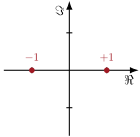
Figure 2: BPSK constellation: the two symbols sit on the real axis, 180 degrees apart
There is another way to change phase 180 degrees, and that’s simply to swap the phase in the transmitter circuit. Imagine as below we have a local oscillator driving pseudo differential common source stages with switches on top. If we flip the switches we can change the phase 180 degrees pretty fast.
A challenge is, however, that the amplitude will change. In general, constant envelope (don’t change amplitude) modulation is less bandwidth efficient (slower) than schemes that change both phase and amplitude.
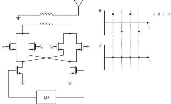
Figure 3: BPSK transmitter: a local oscillator drives a pseudo-differential common source pair, and the $b_0$ switches swap the output phase 180 degrees into the antenna balun
Standards like Zigbee used offset quadrature phase shift keying, with a constellation as shown below. With 4 points we can send 2 bits per symbol.
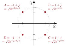
Figure 4: QPSK constellation: four symbols at $\pm 1 \pm j$, or $\sqrt{2}e^{\pm j\pi/4}$, so 2 bits per symbol
In ZigBee, or 802.15.4 as the standard is called, the phase changes is actually done with a constant envelope.
The nice thing about constant envelope is that the radio transmitter can be simple. We don’t need to change the amplitude. If we have a PLL as a local oscillator, where we can change the phase (or frequency), then we only need a power amplifier before the antenna.
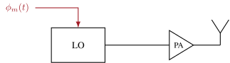
Figure 5: Constant envelope transmitter: the phase is modulated in the local oscillator, and a power amplifier drives the antenna
For phase and amplitude modulation, or complex transmitters, we need a way to change the amplitude and phase. What a shocker. There are two ways to do that. A polar architecture where phase change is done in the PLL, and amplitude in the power amplifier.
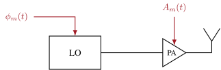
Figure 6: Polar transmitter: phase $\phi$ is modulated in the local oscillator and amplitude $A$ in the power amplifier
Or a Cartesian architecture where we make the in-phase component, and quadrature-phase components in digital, then use two digital to analog converters, and a set of complex mixers to encode onto the carrier. The power amplifier would not need to change the amplitude, but it does need to be linear.
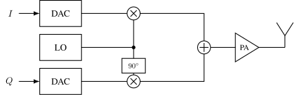
Figure 7: Cartesian transmitter. Two converters produce $I$ and $Q$, two mixers multiply them by copies of the local oscillator ninety degrees apart, and the sum drives a linear power amplifier. The $90^\circ$ block is the whole difference between this and two copies of the same branch: without it both mixers would be multiplying by the same carrier, and the sum would carry no phase information.
We can continue to add constellation points around the unit circle. Below we can see 8-PSK, where we can send 3-bits per symbol. Assuming we could shift position between the constellation points at a fixed rate, i.e 1 mega symbols per second. With 1-bit per symbol we’d get 1 Mbps. With 3-bits per symbol we’d get 3 Mbps.
We could add 16 points, 32 points and so on to the unit circle, however, there is always noise in the transmitter, which will create a cloud around each constellation point, and it’s harder and harder to distinguish the points from each other.
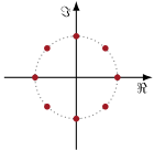
Figure 8: 8-PSK constellation: eight points on the unit circle, so 3 bits per symbol
Bluetooth Classic uses $\pi/4$-DQPSK and 8DPSK.
DPSK means differential phase shift keying. Think about DPSK like this. In the QPSK diagram above the symbols (00,01,10,11) are determined by the constellation point $1 + j$, $1-j$ and so on. What would happen if the constellation rotated slowly? Would $1+j$ turn into $1-j$ at some point? That might screw up our decoding if the received constellation point was at $1 + 0j$, we would not know what it was.
If we encoded the symbols as a change in phase instead (differential), then it would not matter if the constellation rotated slowly. A change from $1+j$ to $1-j$ would still be 90 degrees.
Why would the constellation rotate you ask? Imagine the transmitter transmits at 2 400 000 000 Hz. How does our receiver generate the same frequency? We need a reference and a PLL. The crystal-oscillator reference has a variation of +-50 ppm, so $2.4e9 \times 50/1e6 = 120$ kHz.
Assume our receiver local oscillator was at 2 400 120 000 Hz. The transmitter sends 2 400 000 000 Hz + modulation. At the receiver we multiply with our local oscillator, and if you remember your math, multiplication of two sine creates a sum and a difference between the two frequencies. As such, the low frequency part (the difference between the frequencies) would be 120 kHz + modulation. As a result, our constellation would rotate 120 000 times per second. Assuming a symbol rate of 1MS/s our constellation would rotate roughly 1/10 of the way each symbol.
In DPSK the rotation is not that important. In PSK we have to measure the carrier offset, and continuously de-rotate the constellation.
Most radios will de-rotate somewhat based on the preamble, for example in Bluetooth Low Energy there is an initial 10101010 sequence that we can use to estimate the offset between TX and RX carriers, or the frequency offset.
The $\pi/4$ part of $\pi/4-DQPSK$ just means we actively rotate the constellation 45 degrees every symbol, as a consequence, the amplitude never goes through the origin. In the transmitter circuit, it’s difficult to turn the carrier off, so we try to avoid the zero point in the constellation.
The radio numbers live in the Bluetooth Core Specification: Enhanced Data Rate uses $\pi/4$-DQPSK at 2 Mb/s and 8DPSK at 3 Mb/s.
I don’t think 16PSK is that common, at 4-bits per symbol it’s common to switch to Quadrature Amplitude Modulation (QAM), as shown below. The goal of QAM is to maximize the distance between each symbol. The challenge with QAM is the amplitude modulation. The modulation scheme is sensitive to variations in the transmitter amplitude. As such, more complex circuits than 8PSK could be necessary.
If you wanted to research “new fancy modulation schemes” I’d think about Sphere packing.
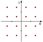
Figure 9: 16-QAM constellation: a 4 by 4 grid of points in phase and amplitude, so 4 bits per symbol
Single carrier, or multi carrier?
Assume we wanted to send 1 Gbps over the air. We could choose a bandwidth of about 1 GHz with 1 bit per symbol, or a bandwidth of 100 MHz if we sent 1024 QAM at 100 MS/s. Both cases would look like the figure below.
In both cases we get problems with the physical communication channel, the change in phase and amplitude affect what is received. For a 1 GHz bandwidth at 2.4 GHz carrier we’d have problems with the phase. At 1024 QAM we’d have problems with the amplitude.

Figure 10: Single carrier link: amplitude $A_m(t)$ and phase $\phi_m(t)$ are modulated onto I and Q, transmitted, and de-modulated after the receiver
Back in 1966 Orthogonal frequency division multiplexing was introduced to deal with the communication channel. In OFDM we modulate a number of sub-carriers in the frequency space with our wanted modulation scheme (BPSK, PSK, QAM), then do an inverse fourier transform to get the time domain signal, mix on to the carrier, and transmit. At the receiver we take an FFT and do demodulation in the frequency space. See example in figure below.
The name “multiple carriers” is a bit misleading. Although there are multiple carriers on the left and right side of the figure, there is normally still just one carrier in the TX/RX.

Figure 11: OFDM link: the sub-carriers are modulated in frequency space, an IFFT makes the time domain I and Q for the transmitter, and an FFT at the receiver recovers the sub-carriers
There are more details in OFDM than the simple statement above, but the details are just to fix challenges, such as “How do I recover the symbol timing? How do I correct for frequency offset? How do I ensure that my time domain signal terminates correctly for every FFT chunk”
The genius with OFDM is that we can pick a few of the sub-carriers to be pilot tones that carry no new information. If we knew exactly what was sent in phase and amplitude, then we could measure the phase and amplitude change due to the physical communication channel, and we could correct the frequency space before we tried to de-modulate.
It’s possible to do the same with single carrier modulation also. Imagine we made a 128-QAM modulation on a single carrier. As long as we constructed the time domain signal correctly (cyclic prefix to make the FFT work nicely, some preamble to measure the communication channel, then we could take an FFT at the receiver, correct the phase and amplitude, do an IFFT and demodulate the time-domain signal as normal.
In radio design there are so many choices it’s easy to get lost.
Use a Software Defined Radio
For our mouse, what radio scheme should we choose? One common instance of “how to make a choice” in industry is “Delay the choice as long as possible so you’re sure the choice is right”.
Maybe the best would be to use a software defined radio receiver? Something like the picture below, an antenna, low noise amplifier, and a analog-to-digital converter. That way we could support any transmitter. Fantastic idea, right?
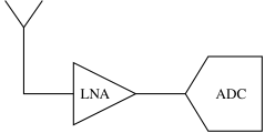
Figure 12: Software defined radio receiver: antenna, low noise amplifier and analog-to-digital converter, nothing else
Well, lets check if it’s a good idea. We know we’ll use 2.4 GHz, so we need about 2.5 GHz bandwidth, at least. We know we want good range, so maybe 100 dB dynamic range. In analog to digital converter design there are figure of merits, so we can actually compute a rough power consumption for such an ADC.
ADC FOM \(= \frac{P}{2 BW 2^n}\)
State of the art FOM \(\approx 5 \text{ fJ/step}\)
\[BW = 2.5\text{ GHz}\] \[DR = 100\text{ dB} \Rightarrow \text{Bits} = (100-1.76)/6.02 \approx 16\text{ bit}\] \[P = 5\text{ fJ/step} \times 5 \text{ GHz} \times 2^{16} = 1.6\text{ W}\]At 1.6 W our mouse would only last for 2 hours. That’s too short. It will never be a low power idea to convert the full 2.5 GHz bandwidth to digital, we need some bandwidth selectivity in the receive chain.
Bluetooth
Bluetooth was made to be a “simple” standard and was introduced in 1998. The standard has continued to develop, with Low Energy introduced in 2010. The latest planned changes can be seen at Specifications in Development.
Bluetooth Basic Rate/Extended Data rate
- 2.400 GHz to 2.4835 GHz
- 1 MHz channel spacing
- 78 Channels
- Up to 20 dBm
- Minimum -70 dBm sensitivity (1 Mbps)
- 1 MHz GFSK (1 Mbps), pi/4-DQPSK (2 Mbps), 8DPSK (3 Mbps)
You’ll find BR/EDR in most audio equipment, cars and legacy devices. For new devices (also audio), there is now a transition to Bluetooth Low Energy.
Bluetooth Low Energy
- 2.400 GHz to 2.480 GHz
- 2 MHz channel spacing
- 40 Channels (3 primary advertising channels)
- Up to 20 dBm
- Minimum -70 dBm sensitivity (1 Mbps)
- 1 MHz GFSK (1 Mbps, 500 kbps, 125 kbps), 2 MHz GFSK (2 Mbps)
Below are the Bluetooth LE channels. The green are the advertiser channels, the blue are the data channels, and the red humps are the WiFi channels.
The advertiser channels have been intentionally placed where there is space between the WiFi channels to decrease the probability of collisions.
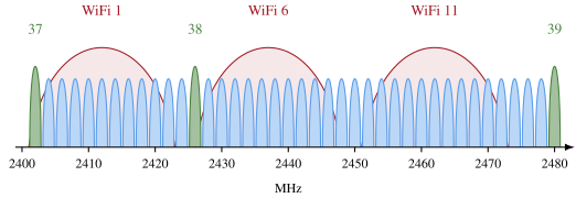
Figure 13: Bluetooth LE channel map: advertising channels 37, 38 and 39 (green) at 2402, 2426 and 2480 MHz sit in the gaps around WiFi channels 1, 6 and 11 (red); the 37 data channels are blue
Any Bluetooth LE peripheral will advertise its presence, it will wake up once in a while (every few hundred milliseconds, to seconds) and transmit a short “I’m here” packet. After transmitting it will wait a bit in receive to see if anyone responds.
A Bluetooth LE central will camp in receive on a advertiser channel and look for these short messages from peripherals. If one is observed, the Central may choose to respond.
Take any spectrum analyzer anywhere, and you’ll see traffic on 2402, 2426, and 2480 MHz.
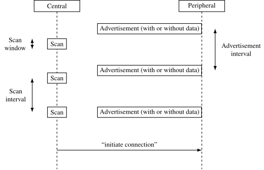
Figure 14: Advertising: the peripheral transmits advertisements once per advertisement interval while the central scans, until the central initiates a connection. Redrawn from Nordic Semiconductor DevZone
In a connection a central and peripheral (the master/slave names below have been removed from the spec, that was a fun update to a 3500 page document) will have agreed on an interval to talk. Every “connection interval” they will transmit and receive data. The connection interval is tunable from 7.5 ms to seconds.
Bluetooth LE is the perfect standard for wireless mice.
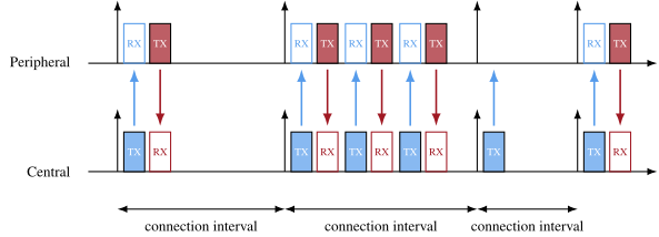
Figure 15: In a connection, central and peripheral exchange transmit and receive packets once every connection interval; an event with no data is still a transmission. Redrawn from Nordic Semiconductor DevZone
further information Building a Bluetooth application on nRF Connect SDK
Bluetooth Specifications in Development
Algorithm to design state-of-the-art LE radio
- Find most recent digest from International Solid State Circuit Conference (ISSCC)
- Find Bluetooth low energy papers
- Pick the best blocks from each paper
A typical Bluetooth radio may look something like the picture below. There would be a single antenna for both RX and Tx. There will be some way to combine the transmit and receive path in a match, or balun.
The receive chain would have a LNA, mixer, anti-alias filter and analog-to-digital converters. It’s likely that the receive path would be complex (in-phase and quadrature phase) after mixer.
There would be a local oscillator (all-digital phase-locked-loop) to provide the frequency to the mixers and transmit path, which could be either polar or Cartesian.
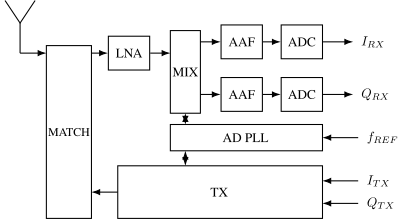
Figure 16: Typical Bluetooth radio: antenna and match, LNA, mixer, I and Q anti-alias filters and ADCs, an all-digital PLL, and the transmit path
In the typical radio we’ll need the blocks below. I’ve added a column for how many people I would want if I was to lead development of a new radio.
| Blocks | Key parameter | Architecture | Complexity (nr people) |
|---|---|---|---|
| Antenna | Gain, impedance | lambda/4 | <1 |
| RF match | loss, input impedance | PI-match | <1 |
| Low noise amp | NF, current, linearity | LNTA | 1 |
| Mixer | NF, current, linearity | Passive | 1 |
| Anti-alias filter | NF, current, linearity | Active-RC | 1 |
| ADC | Sample rate, dynamic range, linearity | NS-SAR | 1 - 2 |
| PLL | Phase noise, current | AD-PLL | 2-3 |
| Baseband | Eb/N0, gate count, current. | SystemVerilog | > 10 |
LNTA
The first thing that must happen in the radio is to amplify the noise as early as possible. Any circuit has inherent noise, be it thermal-, flicker-, burst-, or shot-noise. The earlier we can amplify the input noise, the less contribution there will be from the radio circuits.
The challenges in the low noise amplifier is to provide the right gain. If there is a strong input signal, then reduce the gain. If there is a low input signal, then increase the gain.
One way to implement variable gain is to reconfigure the LNA. For an example, see
30.5 A 0.5V BLE Transceiver with a 1.9mW RX Achieving -96.4dBm Sensitivity and 4.1dB Adjacent Channel Rejection at 1MHz Offset in 22nm FDSOI 1
A typical Low Noise Transconductance Amplifier is seen below. It’s a combination of both a common source, and a common gate amplifier. The current in the NMOS and PMOS is controlled by Vgp and Vgn. Keep in mind that at RF frequencies the signals are weak, so it’s easy to provide the DC for the LNA with a resistor to a diode connected PMOS or NMOS.
In a LNA the input impedance must be matched to what is required by the antenna/match in order to have maximum power transfer, that’s the role of the inductors/capacitors.
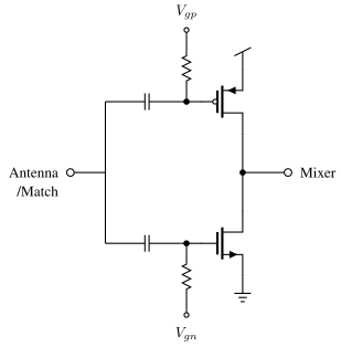
Figure 17: Low noise transconductance amplifier: complementary common source PMOS and NMOS, AC coupled from the antenna match and biased through resistors by $V_{gp}$ and $V_{gn}$
MIXER
In the mixer we multiply the input signal with our local oscillator. Most often a complex mixer is used. There is nothing complex about complex signal processing, just read
Complex signal processing is not complex 2
In order to reduce power, it’s most common with a passive mixer as shown below. A passive mixer is just MOS that we turn on and off with 25% duty-cycle. See example in
A 370uW 5.5dB-NF BLE/BT5.0/IEEE 802.15.4-Compliant Receiver with >63dB Adjacent Channel Rejection at >2 Channels Offset in 22nm FDSOI 3
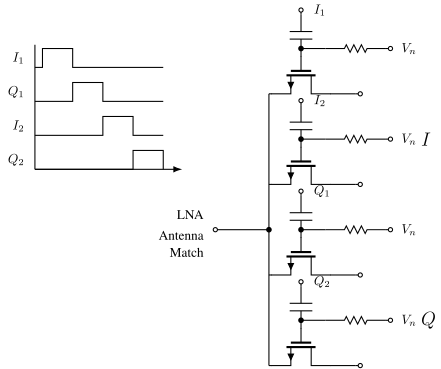
Figure 18: Passive complex mixer: four MOS switches driven by 25% duty-cycle clocks $I_1$, $I_2$, $Q_1$ and $Q_2$ split the LNA current into the I and Q outputs. Each gate is AC coupled to its clock and biased to $V_n$ through a resistor, so the switch sees a rail-to-rail drive while its DC operating point is set independently. Note in the timing diagram that the four phases abut: four quarters fill the period exactly, so between them the switches carry the whole of the LNA current and none of it is thrown away.
To generate the quadrature and in-phase clock signals, which must be 90 degrees phase offset, it’s common to generate twice the frequency in the local oscillator (4.8 GHz), and then divide down to 4 2.4 GHz clock signals.
If the LO is the same as the carrier, then the modulation signal will be at DC, often called direct conversion.
The challenge at DC is that there is flicker noise, offset, and burst noise. The modulation type, however, can impact whether low frequency noise is an issue. In OFDM we can choose to skip the sub-carriers around 0 Hz, and direct conversion works well. An advantage with direct conversion is that there is no “image frequency” and we can use the full complex bandwidth.
For FSK and direct conversion the low frequency noise can cause issues, as such, it’s common to offset the LO from the transmitted signal, for example 4 MHz offset. The low frequency noise problem disappears, however, we now have a challenge with the image frequency (-4 MHz) that must be rejected, and we need an increased bandwidth.
There is no “one correct choice”, there are trade-offs that both ways. KISS (Keep It Simple Stupid) is one of my guiding principles when working on radio architecture.
These days most de-modulation happens in digital, and we need to convert the analog signal to digital, but first AAF.
AAF
The anti alias filter rejects frequencies that can fold into the band of interest due to sampling. A simple active-RC filters is often good enough.
We often need gain in the AAF, as the LNA does not have sufficient gain for the weakest signals. -100 dBm in 50 ohm is 2.2 $\mu$V RMS, while the input range of an ADC may be 1 V. Assume we place the lowest input signal at 0.1 V, so we need a voltage gain of $20\log(0.1/2.2\times 10^{-6}) \approx 93$ dB in the receiver.
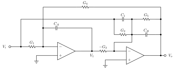
Figure 19: General purpose Active-RC biquad, used here as the anti-alias filter
ADC
Aaah, ADCs, an IP close to my heart. I did my Ph.d and Post-Doc on ADCs, and the Ph.D students I’ve co-supervised have worked on ADCs.
At NTNU there have been multiple students through the years that have made world-class ADCs, and there’s still students at NTNU working on state-of-the-art ADCs.
These days, a good option is a SAR, or a Noise-Shaped SAR.
If I were to pick, I’d make something like A 68 dB SNDR Compiled Noise-Shaping SAR ADC With On-Chip CDAC Calibration 4 as shown in the figure below.
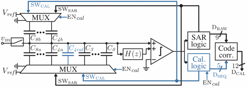
Figure 20: Architecture of the noise-shaping SAR ADC: capacitive DAC with multiplexers, loop filter H(z), integrating comparator, SAR logic, calibration logic and code correction
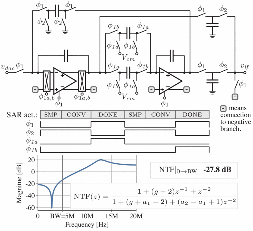
Figure 21: The switched-capacitor loop filter with two OTAs (the first one chopped), the clock phases relative to the SAR activity, and the resulting NTF with -27.8 dB in-band suppression
Or if I did not need high resolution, I’d choose my trusty A Compiled 9-bit 20-MS/s 3.5-fJ/conv.step SAR ADC in 28-nm FDSOI for Bluetooth Low Energy Receivers 5.
The main selling point of that ADC was that it’s compiled from a JSON file, a SPICE file and a technology file into a DRC/LVS clean layout.
I also included a few circuit improvements. The bottom plate of the SAR capacitor is in the clock loop for the comparator (DN0, DP1 below), as such, the delay of the comparator automatically adjusts with capacitance corner, so it’s more robust over corners
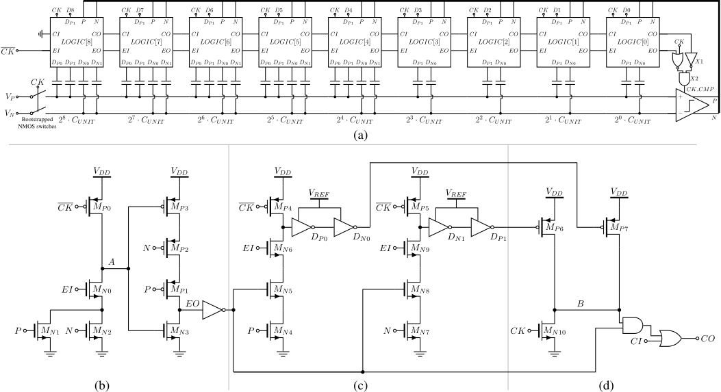
Figure 22: SAR ADC schematic: (a) capacitor array with self-timed SAR logic chain and comparator, (b) enable flip-flop, (c) bottom-plate switching of the CDAC, (d) comparator clock generation
The compiled nature also made it possible to quickly change the transistor technology. Below is a picture with 180 nm FDSOI transistors on the left, and 28 nm FDSOI transistors on the right.
I detest doing anything twice, so I love the fact that I never have to re-draw that ADC again. I just fix the technology file (and maybe some tweaks to the other files), and I have a completed ADC.
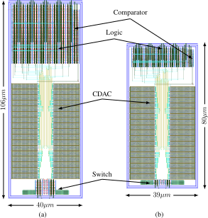
Figure 23: Layout of the two compiled SAR ADCs with comparator, logic, CDAC and switch: (a) 180 nm IO-transistor version, (b) core-transistor version
AD-PLL
The phase locked loop is the heart of the radio, and it’s probably the most difficult part to make. Depends a bit on technology, but these days, All Digital PLLs are cool. Start by reading Razavi’s PLL book.
You can spend your life on PLLs.
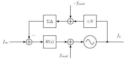
Figure 24: Two-point modulation: the modulation is applied to the oscillator and the opposite signal to the sigma-delta feedback divider, so the loop does not see it
AD-PLL with Bang-Bang phase detector for steady-state
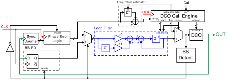
Figure 25: All-digital PLL with a bang-bang phase detector for steady-state: phase error logic, digital loop filter, DCO calibration engine with frequency offset estimator, and steady-state detect
Baseband
Once the signal has been converted to digital, then the de-modulation, and signal fixing start. That’s for another course, but there are interesting challenges.
| Baseband block | Why |
|---|---|
| Mixer? | If we’re using low intermediate frequency to avoid DC offset problems and flicker noise |
| Channel filters? | If the AAF is insufficient for adjacent channel |
| Power detection | To be able to control the gain of the radio |
| Phase extraction | Assuming we’re using FSK |
| Timing recovery | Figure out when to slice the symbol |
| Bit detection | single slice, multi-bit slice, correlators etc |
| Address detection | Is the packet for us? |
| Header detection | What does the packet contain |
| CRC | Does the packet have bit errors |
| Payload de-crypt | Most links are encrypted by AES |
| Memory access | Payload need to be stored until CPU can do something |
What do we really want, in the end?
The receiver part can be summed up in one equation for the sensitivity. The noise in a certain bandwidth. The Noise Figure of the analog receiver. The Energy per bit over Noise of the de-modulator.
\[P_{RX_{sens}} = -174 \text{ dBm} + 10 log_{10}(R_b) + NF + E_b/N_0\]Term by term: $-174$ dBm is the thermal noise in one hertz at room temperature, $R_b$ is the bit rate, which sets how much bandwidth that noise is collected over, $NF$ is what the receiver’s own noise adds, and $E_b/N_0$ is what the demodulator needs to hit its error rate. Note that $R_b$ here is the data rate; earlier in this chapter $DR$ meant dynamic range, which is a different quantity entirely.
The useful move is to run it backwards. The nRF5340 datasheet quotes $-97.5$ dBm sensitivity at 1 Mbps, and $10log_{10}(10^6) = 60$ dB, so
\[P_{RX_{sens}} + 174 - 60 = NF + E_b/N_0 = 16.5 \text{ dB}\]and that 16.5 dB is the entire budget shared between the analog front end and the demodulator. GFSK needs something like 12 dB of $E_b/N_0$, which leaves only a few decibels of noise figure for everything in front of it. That is the number the rest of this chapter is really about.
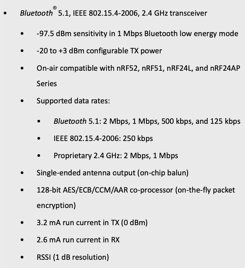
Figure 26: nRF5340 radio specification: -97.5 dBm sensitivity at 1 Mbps Bluetooth LE, 2.6 mA in receive and 3.2 mA in transmit. Source: Nordic Semiconductor, nRF5340 Product Specification
In the block diagram of the device the radio might be a small box, and the person using the radio might not realize how complex the radio actually is.
I hope you understand now that it’s actually complicated.
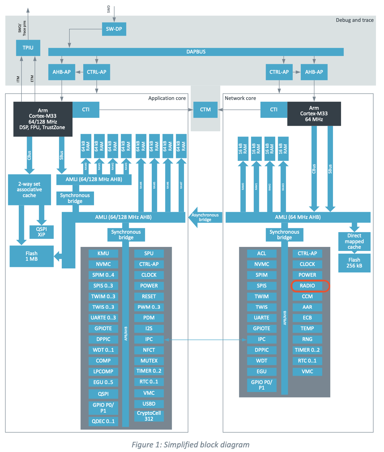
Figure 27: nRF5340 block diagram, where the entire radio is the single RADIO block (circled) in the network core
Summary
The one-page version of this chapter:
- Start from the link budget: Friis in free space, a rather worse exponent indoors, and the antenna wants its fraction of a wavelength
- The ISM bands set the playing field; 2.4 GHz trades antenna size against propagation and company
- Energy per bit is the real currency: modulation choice, data rate and duty cycle set the average current, and the battery sets the lifetime
- Single-carrier modulation keeps the PA efficient (constant envelope); multi-carrier buys spectral efficiency at the cost of backoff
- The receive chain is LNA, mixer and filter: the LNA sets the noise figure, the mixer moves the band, and everything after runs at a friendlier frequency
- A software-defined radio on the bench teaches more about radios than any equation in this chapter
Would you like to know more?
A 0.5V BLE Transceiver with a 1.9mW RX Achieving -96.4dBm Sensitivity and 4.1dB Adjacent Channel Rejection at 1MHz Offset in 22nm FDSOI 1, M. Tamura, Sony Semiconductor Solutions, Atsugi, Japan, 30.5, ISSCC 2020
A 370uW 5.5dB-NF BLE/BT5.0/IEEE 802.15.4-Compliant Receiver with >63dB Adjacent Channel Rejection at >2 Channels Offset in 22nm FDSOI 3, B. J. Thijssen, University of Twente, Enschede, The Netherlands
A 68 dB SNDR Compiled Noise-Shaping SAR ADC With On-Chip CDAC Calibration 4, H. Garvik, C. Wulff, T. Ytterdal
A Compiled 9-bit 20-MS/s 3.5-fJ/conv.step SAR ADC in 28-nm FDSOI for Bluetooth Low Energy Receivers 5, C. Wulff, T. Ytterdal
Cole Nielsen, https://github.com/nielscol/thesis_presentations
“Python Framework for Design and Simulation of Integer-N ADPLLs”, Cole Nielsen, https://github.com/nielscol/tfe4580-report/blob/master/report.pdf
Design of CMOS Phase-Locked Loops 6, Behzad Razavi, University of California, Los Angeles
-
M. Tamura and H. Takano and S. Shinke and H. Fujita and H. Nakahara and N. Suzuki and Y. Nakada and Y. Shinohe and S. Etou and T. Fujiwara and Y. Katayama, 30.5 A 0.5V BLE Transceiver with a 1.9mW RX Achieving $-$96.4dBm Sensitivity and 4.1dB Adjacent Channel Rejection at 1MHz Offset in 22nm FDSOI 2020 https://doi.org/10.1109/ISSCC19947.2020.9063021 ↩ ↩2
-
K. Martin, Complex signal processing is not complex 2004 https://doi.org/10.1109/TCSI.2004.834522 ↩
-
B. J. Thijssen and E. A. M. Klumperink and P. Quinlan and B. Nauta, 30.4 A 370$\mu$W 5.5dB-NF BLE/BT5.0/IEEE 802.15.4-Compliant Receiver with >63dB Adjacent Channel Rejection at >2 Channels Offset in 22nm FDSOI 2020 https://doi.org/10.1109/ISSCC19947.2020.9062973 ↩ ↩2
-
Garvik, Harald and Wulff, Carsten and Ytterdal, Trond, A 68 dB SNDR Compiled Noise-Shaping SAR ADC With On-Chip CDAC Calibration 2019 https://doi.org/10.1109/A-SSCC47793.2019.9056925 ↩ ↩2
-
Wulff, Carsten and Ytterdal, Trond, A Compiled 9-bit 20-MS/s 3.5-fJ/conv.step SAR ADC in 28-nm FDSOI for Bluetooth Low Energy Receivers 2017 https://doi.org/10.1109/JSSC.2017.2685463 ↩ ↩2
-
B. Razavi, Design of CMOS Phase-Locked Loops 2020 https://doi.org/10.1017/9781108626200 ↩