Table of contents
Keywords: Resistors, Polysilicon, Diffusion, Capacitors, MOM, MOS Cap, Varactors, Inductors
Metal in ICs is not wire in schematic
Metal wires in an integrated circuit come in two types, copper and aluminium.
Most of the routing layers will be copper. To ensure that the copper ions don’t diffuse into the silicon-oxide a barrier material surrounds all copper interconnect.
Copper is too stiff to be wire-bonded. As such, the top layer metals would be aluminium.
Since the routing is so small, we have to care about the parasitic properties of the routing. Below is a table with some common quantities for copper. For example, if we have 1000 $\mu$m metal wire with 1 $\mu$m width, then it would be approximately 150 $\Omega$, 1 nH , 1 pF and tolerate a maximum of 1 mA DC current.
| Parameter | Typ. Value | Unit |
|---|---|---|
| Resistance | 150 | \(\text{m}\Omega/\square\) |
| Capacitance | 1 | \(\text{fF}/\mu\text{m}\) |
| Inductance | 1 | nH/mm |
| Max DC current | 1 | mA/\(\square\) |
The type of circuit we have determines what we must simulate. Everything needs to be simulated with parasitic capacitance and max current. Analog and power circuits need parasitic resistance as well; only RF and power usually need the inductance too.
| Circuit type | Must simulate/know |
|---|---|
| All | C Imax |
| Analog, Power | R C Imax |
| Some RF, Some Power | R L C Imax |
To simulate the effects of parasitics, we need a description of the technology. A Process Design Kit (PDK). Most PDKs are closely guarded secrets, as they describe many things about the way the foundry makes the integrated circuits.
Some PDKs are open source, however, see Skywater 130 nm and IHP-Open-PDK
In addition to the PDK, we need tools that can calculate from the layout the parasitic elements. Some of the tools are
Layout parasitic extraction tools
3D EM Simulators
Transistor CAD (TCAD)
Resistors
Sometimes we want a specific resistance. In general, any resistance on IC will vary in absolute value by maybe up to $\pm$ 20 %. The relative size, however, can be controlled to within 0.1 %.
In other words, you can’t rely on a 1 kOhm resistor actually being 1 kOhm, it might be 0.8 kOhm. If you have two, however, you can trust that both of them will be 0.8 kOhm.
That’s why almost all analog circuits rely on the relative sizes of passives, not the absolute value. If a circuit does rely on absolute values, then it usually needs to be trimmed in production.
Polysilicon
The workhorse resistor is the gate material itself: polysilicon. In Figure 1 the resistor is a strip of poly with contacts at both ends, sitting on field oxide so it is insulated from the substrate.
Can be both N-doped, and P-doped
Often with two flavors, with, and without silicide
Silicide reduces resistance of polysilicon
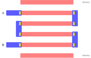
Figure 1: Polysilicon resistor
In a modern process the poly on top of transistors is silicided - a metal alloy on the surface that reduces the sheet resistance to a few ohms per square, great for gates, useless for resistors. The foundry therefore offers a mask that blocks the silicide, and the unsilicided flavor has a sheet resistance of hundreds of ohms per square with a small temperature coefficient. When an analog schematic says “resistor”, it is nearly always unsilicided poly.
Diffusion
A doped region in the silicon also conducts, and Figure 2 shows it used as a resistor.
Use doped region as resistor
Usually without silicide
Non-linear capacitance
Tricky temperature dependence
The diffusion resistor comes with baggage. The resistor body forms a pn junction to whatever surrounds it, so it carries a distributed, voltage dependent junction capacitance, and the depletion region eats into the conducting cross section, so the resistance itself moves with the voltage. The substrate is p- in every modern process, so an n+ resistor sits straight in it, but a p+ resistor needs an n-well around it - and that well is a third terminal you must bias, with its own junction to the substrate underneath. Add a temperature coefficient set by doping and mobility pulling in opposite directions, and the diffusion resistor is a device you use when the poly resistor is unavailable, not because you want to.
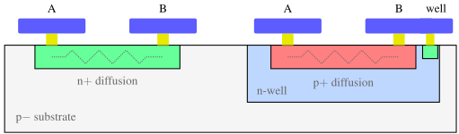
Figure 2: Diffusion resistors: n+ in the substrate, p+ in an n-well
Metal
Metal, Figure 3, is at the other end of the scale: at milliohms per square you would need a kilometer of it for a useful resistance.
Usually too low ohmic to be a useful resistor
Useful for “separating nets” in schematic and layout
Must be considered for power supply and ground routing (high currents)
A zero ohm metal “resistor” still earns its place in the schematic: it splits a net in two, which lets layout tools keep sense lines away from current carrying lines, and lets the extraction report where the IR drop goes. In power routing the metal resistance is not a device you add but a parasitic you budget: milliohms times amperes is millivolts of ground bounce.
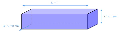
Figure 3: Metal resistor
Capacitors
What is S, M, L, XL on a chip?
Capacitors are where the silicon area goes, so before the devices, a sense of scale. The nRF52832 die is about 9.6 million square micrometers, and on it, a component below five thousand square micrometers is small, while anything above two hundred thousand - a fiftieth of the die - is extra large and had better earn its keep.
nRF52832 \(3200 \mu m \times 3000 \mu m = 9600 k \mu m^2\)
| Size | Area |
|---|---|
| S | below 5 k square um |
| M | below 50 k square um |
| L | below 200 k square um |
| XL | above 200 k square um |
Metal-Oxide-Metal finger capacitors
The default capacitor in a modern process is drawn, not grown: thin metal fingers side by side, alternating polarity, stacked over several metal layers, as in Figure 4. The lateral spacing between fingers is smaller than the vertical oxide between layers, so the sideways fringe field does most of the work.
Unit capacitance \(\approx 1 fF/\mu m^2/layer\)
\[10 pF = 100 \mu m \times 100 \mu m = 10 k \mu m^2\]
Figure 4: Metal-oxide-metal finger capacitor
The MOM capacitor is linear, matches to a tenth of a percent when drawn as identical units, and costs nothing but metal. Its weakness is density: at about a femtofarad per square micrometer per layer, ten picofarads is a hundred micrometers on a side - a Medium on the scale above, for one capacitor.
MOS capacitors
When density matters more than linearity, use the thinnest oxide on the die: the gate oxide. A MOSFET with source, drain and bulk tied together is a capacitor from the gate to the channel, Figure 5, and it is about ten times denser than the MOM capacitor.
The price is that the capacitance depends on the bias. Below threshold there is no channel and the gate sees the oxide in series with the depletion region; above threshold the inversion layer forms and the capacitance jumps to the full oxide value. A MOS capacitor is a fine decoupling capacitor - the bias is fixed and nobody cares about linearity - and a poor filter capacitor.
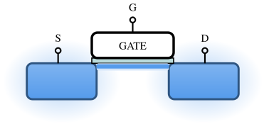
Figure 5: A MOS capacitor is a MOSFET in strong inversion
dicex/sim/spice/NCHIO/vcap.cir
* gate cap

.include ../../../models/ptm_130.spi

vdrain D 0 dc 1
vgaini G 0 dc 0.5
vbulk B 0 dc 0
vcur S 0 dc 0

M1 D G S B nmos  w=1u  l=1u

.op
The operating point readout below, from the SPICE deck on the left, shows where the number comes from: at this bias the gate-gate capacitance $C_{gg}$ of the 1 um by 1 um device reads about 10 fF - ten femtofarads per square micrometer, right at the estimate.
Moscap is \(\approx 10 fF / \mu m^2\)
\[10 pF = 31 \mu m \times 31 \mu m \approx 1 k \mu m^2\]dicex/sim/spice/NCHIO/vcap.vlog
Device m1:
Vgs (gate-source voltage) [V] : 0.5
Vgd (gate-drain voltage) [V] : -0.5
Vds (drain-source voltage) [V] : 1
Vbs (bulk-source voltage) [V] : 1.90808e-12
Vbd (bulk-drain voltage) [V] : -1
Id (drain current) [A] : 7.32634e-06
Is (source current) [A] : -7.32633e-06
Ibd (bulk-drain current) [A] : -1.01e-12
Ibs (bulk-source current) [A] : 9.581e-25
Vt (threshold voltage) [V] : 0.378198
Vgt (gate overdrive voltage) [V] : 0.121802
Vgsteff (effective vgt) [V] : 0.12515
Gm (transconductance) [S] : 8.44164e-05
Gmb (bulk bias transconductance) [S] : 2.00071e-05
Ueff (mobility) [cm^2/Vs] : 417.675
Gds (channel conductance) [S] : 1.95043e-07
Rds (output resistance) [Ohm] : 5.12708e+06
Vdsat (drain saturation voltage) [V] : 0.14171
IC (inversion coefficient) [] : 4.42478
Cgs (gate-source capacitance) [F] : 9.98457e-15
Csg (source-gate capacitance) [F] : 5.86932e-15
Cgd (gate-drain capacitance) [F] : 3.98239e-16
Cdg (drain-gate capacitance) [F] : 3.91086e-15
Cds (drain-source capacitance) [F] : 4.30968e-15
Cgg (gate-gate capacitance) [F] : 1.05198e-14
Cdd (drain-drain capacitance) [F] : 1.05198e-14
Css (source-source capacitance) [F] : 0
Cgb (gate-bulk capacitance) [F] : 1.05198e-14
Cbg (bulk-gate capacitance) [F] : 1.74123e-15
Cbs (bulk-source capacitance) [F] : 8e-16
Cbd (bulk-drain capacitance) [F] : 3.97768e-16
Varactors
A varactor is a “variable capacitor”, usually it’s a device that varies the capacitance with the voltage across the device.
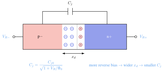
Figure 6: A reverse biased pn junction as a varactor
The junction depletion capacitance falls as the reverse bias grows - the same square root we met in the diode chapter - which makes a reverse biased junction a voltage controlled capacitor. The other common varactor is the MOS capacitor biased around its transition. The customer for both is the oscillator chapter: a varactor in an LC tank turns a fixed oscillator into a voltage controlled one.
Inductors
Inductors on chip are spirals in the top metals, like the ones visible on the nRF51822 die photograph in Figure 7. The top layers are the thick, low resistance ones, and resistance is the enemy: the quality factor of an integrated inductor - some tens at gigahertz - is set by the metal losses and by eddy currents in the substrate below.
Usually two top metals, because they are thick (low ohmic)
Use foundry model
3D electro magnetic simulation often needed
An inductor is the least portable device on the die: its value and its losses depend on everything nearby, so use the foundry’s characterized model, and if the layout deviates from it - or the frequency is high enough that every via matters - budget for a 3D electromagnetic simulation. Nanohenries cost hundreds of micrometers on a side, which is why inductors only appear where nothing else will do: LC oscillators, RF matching and power converters.

Figure 7: nRF51822 die - the spirals are inductors. Die photograph by zeptobars.com, CC BY 3.0
Variation in passives
The rule from the resistor introduction deserves numbers. Nothing on an IC has a trustworthy absolute value: oxide thickness, implant dose and line width all drift from lot to lot, and the passives drift with them. What the process does guarantee is that two identical devices drawn next to each other drift together.
Absolute value for resistors and capacitors: 10 % to 20 %
Relative precision for closely spaced devices: 0.1 % to 1 %
Relative precision for devices far apart on the same die: worse than 2 %
Relative precision
Figure 8 shows the payoff in circuit form: a resistor divider whose output is half the input to a tenth of a percent, and two capacitors whose charge ratio holds equally well - even though every one of those devices may be off by ten percent in absolute value. The precision is earned in layout: identical unit devices, interdigitated or common centroid so process gradients hit both halves equally, dummies at the edges so every unit sees the same neighborhood.
This is the deal the whole chapter has been building to: design circuits so that only ratios matter - two resistors setting a gain, a capacitor array setting a DAC - and the process variation cancels out of the equation.
Resistors and Capacitors can be matched extremely well
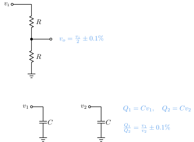
Figure 8: Ratios of matched devices hold to a tenth of a percent
Summary
The one-page version of this chapter:
- Metal is not a schematic wire: budget resistance, capacitance and current for every long route
- Resistors: unsilicided poly first; diffusion if you must; metal never
- Capacitors: MOM for linearity and matching, MOS cap for density at a fixed bias
- Varactors turn junctions or MOS caps into tunable capacitors for oscillators
- Inductors are area-hungry and non-portable: foundry model or EM simulation
- Absolute values drift by tens of percent; ratios of matched units hold a tenth of a percent - design with ratios
Would you like to know more?
Your own PDK documentation is the real reading here: what each resistor, capacitor and inductor in SKY130 actually is, and what it costs in area and parasitics
The circuit-level consequences, chapter by chapter 1
-
David Johns and Ken Martin, Analog Integrated Circuit Design 1997 ; ↩