| Parameter | Typ. Value | Unit |
|---|---|---|
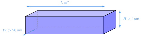
| Resistance | 150 | \(\text{m}\Omega/\square\) |
| Capacitance | 1 | \(\text{fF}/\mu\text{m}\) |
| Inductance | 1 | nH/mm |
| Max DC current | 1 | mA/\(\square\) |

| Circuit type | Must simulate/know |
|---|---|
| All | C Imax |
| Analog, Power | R C Imax |
| Some RF, Some Power | R L C Imax |
Layout parasitic extraction tools
Can be both N-doped, and P-doped
Often with two flavors, with, and without silicide
Silicide reduces resistance of polysilicon
Use doped region as resistor
Usually without silicide
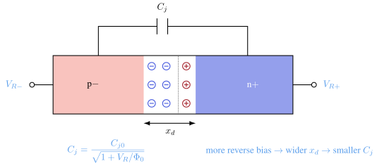
Non-linear capacitance
Tricky temperature dependence
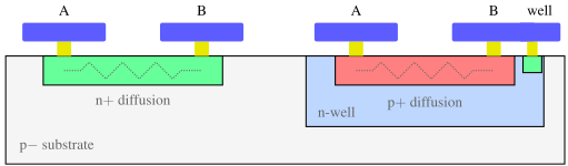
Usually too low ohmic to be a useful resistor
Useful for "separating nets" in schematic and layout
Must be considered for power supply and ground routing (high currents)
nRF52832 \(3200 \mu m \times 3000 \mu m = 9600 k \mu m^2\)
| Size | Area |
|---|---|
| S | below 5 k square um |
| M | below 50 k square um |
| L | below 200 k square um |
| XL | above 200 k square um |
Unit capacitance \(\approx 1 fF/\mu m^2/layer\)
\[10 pF = 100 \mu m \times 100 \mu m = 10 k \mu m^2\]
dicex/sim/spice/NCHIO/vcap.cir
* gate cap
.include ../../../models/ptm_130.spi
vdrain D 0 dc 1
vgaini G 0 dc 0.5
vbulk B 0 dc 0
vcur S 0 dc 0
M1 D G S B nmos w=1u l=1u
.op
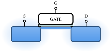
Moscap is \(\approx 10 fF / \mu m^2\)
\[10 pF = 31 \mu m \times 31 \mu m \approx 1 k \mu m^2\]
dicex/sim/spice/NCHIO/vcap.vlog
Device m1:
Vgs (gate-source voltage) [V] : 0.5
Vgd (gate-drain voltage) [V] : -0.5
Vds (drain-source voltage) [V] : 1
Vbs (bulk-source voltage) [V] : 1.90808e-12
Vbd (bulk-drain voltage) [V] : -1
Id (drain current) [A] : 7.32634e-06
Is (source current) [A] : -7.32633e-06
Ibd (bulk-drain current) [A] : -1.01e-12
Ibs (bulk-source current) [A] : 9.581e-25
Vt (threshold voltage) [V] : 0.378198
Vgt (gate overdrive voltage) [V] : 0.121802
Vgsteff (effective vgt) [V] : 0.12515
Gm (transconductance) [S] : 8.44164e-05
Gmb (bulk bias transconductance) [S] : 2.00071e-05
Ueff (mobility) [cm^2/Vs] : 417.675
Gds (channel conductance) [S] : 1.95043e-07
Rds (output resistance) [Ohm] : 5.12708e+06
Vdsat (drain saturation voltage) [V] : 0.14171
IC (inversion coefficient) [] : 4.42478
Cgs (gate-source capacitance) [F] : 9.98457e-15
Csg (source-gate capacitance) [F] : 5.86932e-15
Cgd (gate-drain capacitance) [F] : 3.98239e-16
Cdg (drain-gate capacitance) [F] : 3.91086e-15
Cds (drain-source capacitance) [F] : 4.30968e-15
Cgg (gate-gate capacitance) [F] : 1.05198e-14
Cdd (drain-drain capacitance) [F] : 1.05198e-14
Css (source-source capacitance) [F] : 0
Cgb (gate-bulk capacitance) [F] : 1.05198e-14
Cbg (bulk-gate capacitance) [F] : 1.74123e-15
Cbs (bulk-source capacitance) [F] : 8e-16
Cbd (bulk-drain capacitance) [F] : 3.97768e-16
Usually two top metals, because they are thick (low ohmic)
Use foundry model
3D electro magnetic simulation often needed

Absolute value for resistors and capacitors: 10 % to 20 %
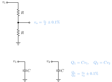
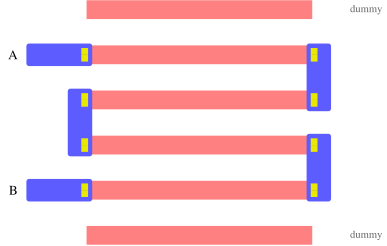
Relative precision for closely spaced devices: 0.1 % to 1 %
Relative precision for devices far apart on the same die: worse than 2 %
Resistors and Capacitors can be matched extremely well