Table of contents
- CMOS Logic
- Analog transistor to digital transistor
- CMOS static logic assumptions
- Don’t break rules unless you know exactly why it will be OK
- Logic cells
- SR-Latch
- D-Latch (16 transistors)
- Other logic cells
- AOI22: and or invert
- Tristate inverter
- Mux
- There are other types of logic
- Speed
- Flip-flops and speed
- Timing analysis
- Timing analysis tools
- Every gate must be simulated to provide behavior over input transition and load capacitance
- All analog blocks must have associated liberty file to describe behavior and timing paths If you integrate analog into digital top flow
- Gate Delay
- Delay estimation
- Elmore Delay
- Delay components
- Modern IC timing analysis requires computers with advanced programs
- Best number of stages
- Which has shortest delay?
- Trends
- Attack vector
- Pick two
- Power
- What is power?
- Power dissipated in a resistor
- Charging a capacitor to VDD
- Energy to charge a capacitor to a voltage VDD
- Discharging a capacitor to 0
- Power consumption of digital circuits
- Sources of power dissipation in CMOS logic
- Switching Power in logic gates
- Switching probability
- Strategies to reduce dynamic power
- Wires
- Wire geometry
- Metal stack
- Metal routing rules on IC
- Modeling Interconnect
- Lumped model
- Wire resistance
- Most wires: Copper
- Contacts
- Wire Capacitance
- FSM
- Mealy machine
- Moore machine
- Mealy versus Moore
- Battery charger FSM
- Summary
- Would you like to know more?
CMOS Logic
Keywords: CMOS Logic, Inverter, NAND, Static Logic, SR-Latch, D-Latch, Flip-Flop, Tristate, AOI
Analog transistor to digital transistor
NMOS current (W = 0.4u L=0.15u) as a function of \(V_{GS}\) and \(V_{DS}\)
dicex/lectures/l13/mos.py
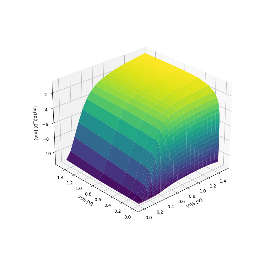
Figure 1: NMOS drain current on a log10 scale as a surface over gate-source and drain-source voltage, for W = 0.4u and L = 0.15u 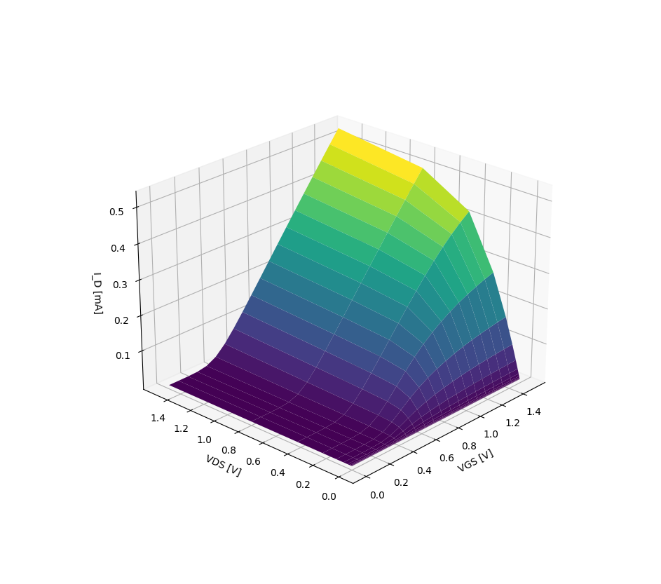
Figure 2: The same NMOS drain current on a linear scale in mA over gate-source and drain-source voltage
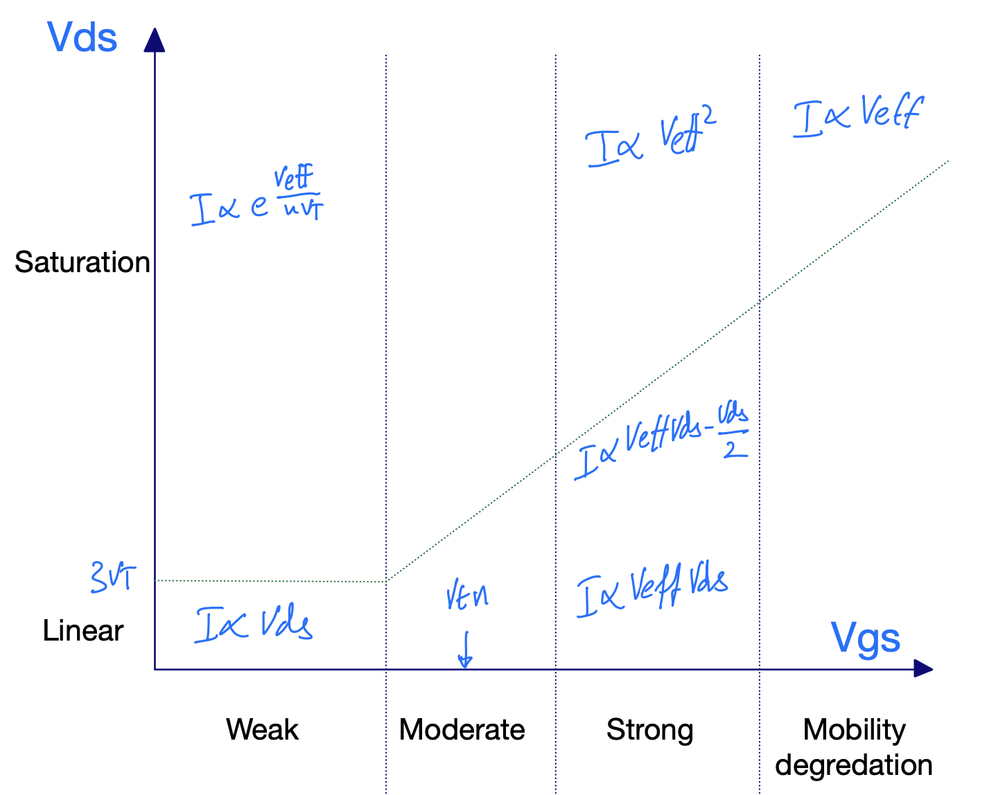
Figure 3: The analog view of the NMOS: current equations for the linear and saturation regions across weak, moderate and strong inversion and mobility degradation
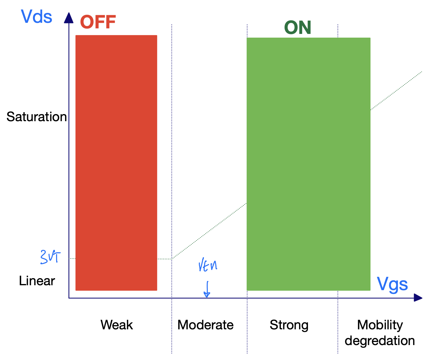
Figure 4: The digital view of the same plane, where weak inversion is treated as OFF and strong inversion as ON, and everything else is ignored
| Gate | NMOS | PMOS |
|---|---|---|
| VDD | ON | OFF |
| VDD -> VSS | X | X |
| VSS -> VDD | X | X |
| VSS | OFF | ON |
| Gate | NMOS | PMOS |
|---|---|---|
| 1 | ON | OFF |
| 1 -> 0 | X | X |
| 0 -> 1 | X | X |
| 0 | OFF | ON |
CMOS static logic assumptions
NMOS source is connected to low potential
\(V_{GS} > V_{TH}\) when \(V_G = V_{DD}\)
PMOS source is connected to high potential
\(V_{GS} < V_{TH}\) when \(V_G = 0\)
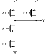
Figure 5: Transistor schematic of a two input NAND, with PMOS A and B in parallel to the supply and NMOS A and B in series to ground
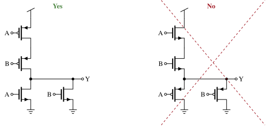
Figure 6: Two ways to wire a NOR - the accepted one with PMOS pulling up and NMOS pulling down, and the rejected one with the device types swapped so the sources sit at the wrong rail
Don’t break rules unless you know exactly why it will be OK
Logic cells
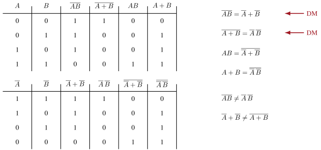
Figure 7: Truth tables for NAND, NOR, AND and OR with inverted inputs, illustrating the two De Morgan identities
CMOS static logic is inverting
| A | Y |
|---|---|
| 1 | 0 |
| 0 | 1 |
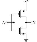
Figure 8: Transistor schematic of the CMOS inverter, one PMOS to the supply and one NMOS to ground sharing gate A and output Y
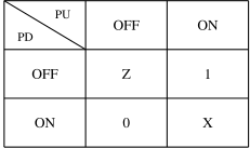
Figure 9: Output state as a function of the pull-up and pull-down networks - Z when both are off, 1 or 0 when one conducts, and X when both conduct
PD = Pull-down PU = Pull-up
logic => [0,1,Z,X];
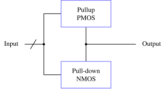
Figure 10: Block view of a static CMOS gate, where the inputs drive a PMOS pull-up network and an NMOS pull-down network that share the output node
Pull-up series
| A | B | Y |
|---|---|---|
| 0 | 0 | 1 |
| 0 | 1 | Z |
| 1 | 0 | Z |
| 1 | 1 | Z |
Pull-up parallel
| A | B | Y |
|---|---|---|
| 0 | 0 | 1 |
| 0 | 1 | 1 |
| 1 | 0 | 1 |
| 1 | 1 | Z |
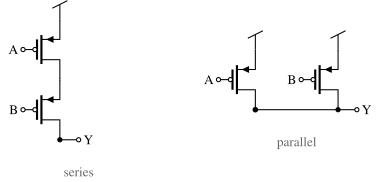
Figure 11: PMOS pull-up networks - two devices in series conduct only when both A and B are 0, two in parallel conduct unless both are 1
Pull-down series
| A | B | Y |
|---|---|---|
| 0 | 0 | Z |
| 0 | 1 | Z |
| 1 | 0 | Z |
| 1 | 1 | 0 |
Pull-down parallel
| A | B | Y |
|---|---|---|
| 0 | 0 | Z |
| 0 | 1 | 0 |
| 1 | 0 | 0 |
| 1 | 1 | 0 |
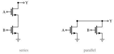
Figure 12: NMOS pull-down networks - two devices in series conduct only when both A and B are 1, two in parallel conduct when either is 1
Rules for inverting logic
Pull-up OR => PMOS in series => POS AND => PMOS in parallel => PAP
Pull-down OR => NMOS in parallel => NOP AND => NMOS in series => NAS
Figure 13: The same pull-up and pull-down blocks, read through the rules that OR maps to PMOS in series and NMOS in parallel, AND to PMOS in parallel and NMOS in series
\[\text{Y} = \overline{\text{AB}} = \text{NOT ( A AND B)}\]AND PU => PMOS in parallel PD => NMOS in series
Figure 14: NAND built from the AND rule, with PMOS A and B in parallel for the pull-up and NMOS A and B in series for the pull-down
| A | B | NOT(A AND B) |
|---|---|---|
| 0 | 0 | 1 |
| 0 | 1 | 1 |
| 1 | 0 | 1 |
| 1 | 1 | 0 |
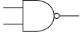
Figure 15: Schematic symbol for the two input NAND gate
\[\text{Y} = \overline{\text{A + B}} = \text{NOT ( A OR B)}\]OR PU => PMOS in series PD => NMOS in parallel
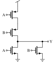
Figure 16: NOR built from the OR rule, with PMOS A and B in series for the pull-up and NMOS A and B in parallel for the pull-down
| A | B | NOT(A OR B) |
|---|---|---|
| 0 | 0 | 1 |
| 0 | 1 | 0 |
| 1 | 0 | 0 |
| 1 | 1 | 0 |
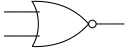
Figure 17: Schematic symbol for the two input NOR gate
SR-Latch
Use boolean expressions to figure out how gates work.
Remember De-Morgan
\(\overline{AB} = \overline{A}+ \overline{B}\) \(\overline{A+B} = \overline{A} \cdot \overline{B}\)
\[Q = \overline{R \overline{Q}} = \overline{R} + \overline{\overline{Q}} = \overline{R} + Q\] \[\overline{Q} = \overline{S Q} = \overline{S} + \overline{Q} = \overline{S} + \overline{Q}\]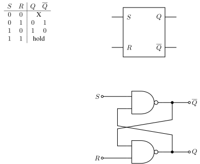
Figure 18: SR-latch truth table and symbol, and the cross-coupled NAND implementation
\(Q = \overline{R} + Q\) ,
\[\overline{Q} =\overline{S} + \overline{Q}\]| S | R | Q | ~Q |
|---|---|---|---|
| 0 | 0 | X | X |
| 0 | 1 | 0 | 1 |
| 1 | 0 | 1 | 0 |
| 1 | 1 | Q | ~Q |
D-Latch (16 transistors)
| C | D | Q | ~Q |
|---|---|---|---|
| 0 | X | Q | ~Q |
| 1 | 0 | 0 | 1 |
| 1 | 1 | 1 | 0 |
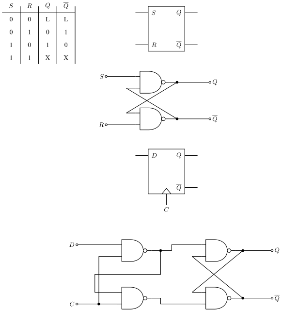
Figure 19: Gate level D latch built from NAND gates, with the cross-coupled NAND SR latch and its truth table above and the full latch driven by clock C below
Other logic cells
What about \(\text{Y} = \text{AB}\) and \(\text{Y} = \text{A} + \text{B}\)?
\[\text{Y} = \text{AB} = \overline{\overline{\text{AB}}}\]Y = A AND B = NOT( NOT( A AND B ) )

Figure 20: An AND gate built as a NAND followed by an inverter
\[\text{Y} = \text{A+B} = \overline{\overline{\text{A+B}}}\]Y = A OR B = NOT( NOT( A OR B ) )

Figure 21: An OR gate built as a NOR followed by an inverter
AOI22: and or invert
Y = NOT( A AND B OR C AND D)
\[\text{Y} = \overline{\text{AB} + \text{CD}}\]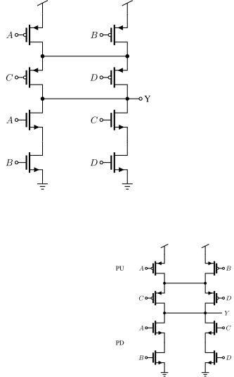
Figure 22: AOI22 gate at transistor level, with the series-parallel pull-up network above the output and the pull-down network below
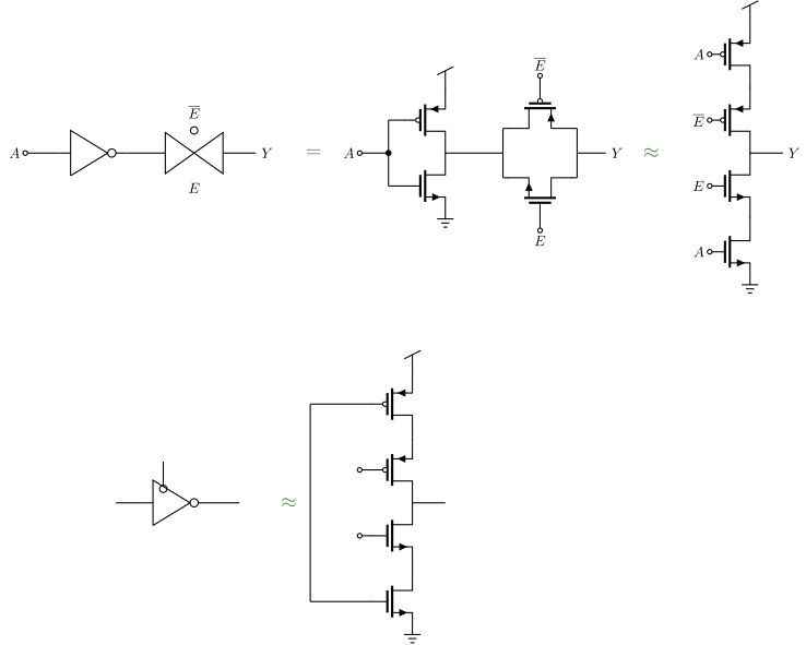
Figure 23: An inverter followed by a transmission gate is equivalent to a tristate inverter, redrawn as a single stack of four series transistors
Tristate inverter
| E | A | Y |
|---|---|---|
| 0 | 0 | Z |
| 0 | 1 | Z |
| 1 | 0 | 1 |
| 1 | 1 | 0 |
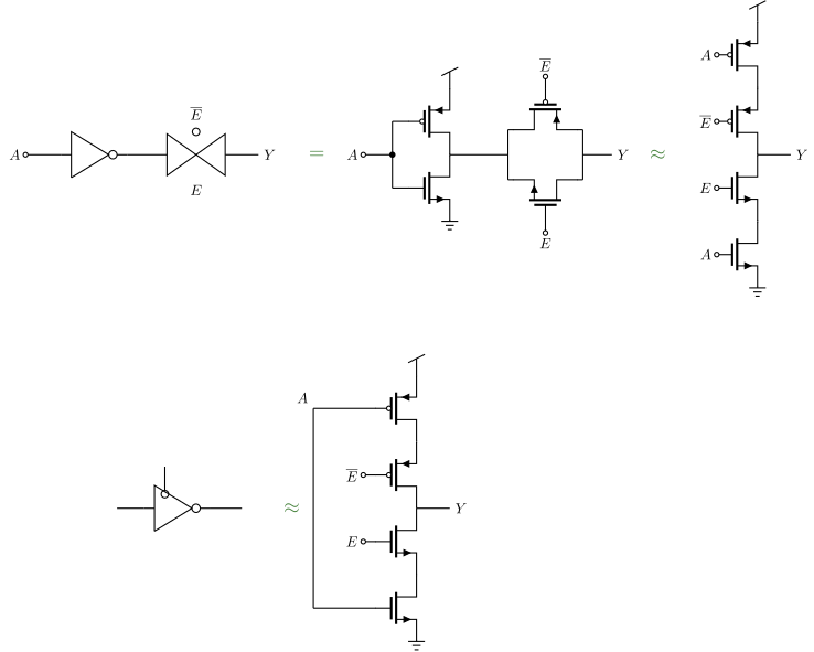
Figure 24: Tristate inverter - symbol and the four transistor stack where input A drives the outer devices and the enable E and its complement drive the inner devices
Mux
| S | Y |
|---|---|
| 0 | NOT(P1) |
| 1 | NOT(P0) |
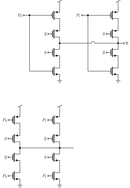
Figure 25: Two input multiplexer built from two tristate inverters, with select S and its complement steering either P0 or P1 to output Y
D-Latch (12 transistors)
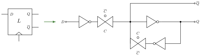
Figure 26: Twelve transistor D latch - input inverter, clocked transmission gate and a feedback inverter pair holding the state, shown as symbol, gate level and transistor level
D-Flip Flop (< 26 transistors)
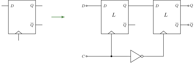
Figure 27: D flip-flop drawn as two D latches in series clocked on opposite phases of C
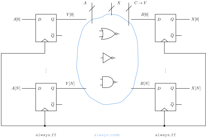
Figure 28: Synchronous digital design, with clocked flip-flop banks at the input and output and a cloud of combinational logic between them
There are other types of logic
- True single phase clock (TSPC) logic
- Pass transistor logic
- Transmission gate logic
- Differential logic
- Dynamic logic
Consider other types of logic “rule breaking”, so you should know why you need it.
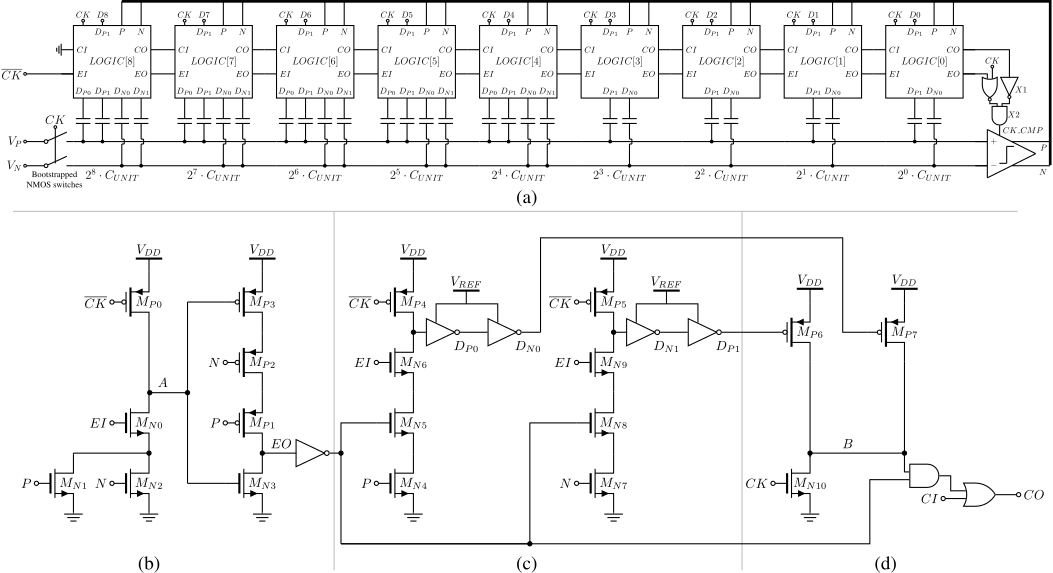
Figure 29: Dynamic logic in a 9-bit SAR ADC - the binary weighted capacitor array with per-bit logic slices above, and the transistor level dynamic cells below
Dynamic logic => A Compiled 9-bit 20-MS/s 3.5-fJ/conv.step SAR ADC in 28-nm FDSOI for Bluetooth Low Energy Receivers 1
Speed
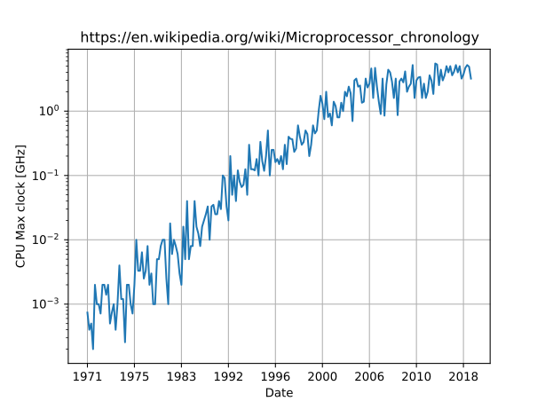
Figure 30: Maximum microprocessor clock frequency in GHz plotted against year from 1971 to 2018, on a logarithmic axis
Figure 31: The same flip-flop and combinational logic structure, whose maximum clock rate is set by the delay through the logic between two flip-flops
Flip-flops and speed
Figure 32: D flip-flop as two cascaded latches, alongside the SPICE subcircuit of the DFRNQNX1 standard cell that implements it
dicex/lib/SUN_TR_GF130N.spi:

.SUBCKT DFRNQNX1_CV D CK RN Q QN AVDD AVSS
XA0 AVDD AVSS TAPCELLB_CV
XA1 CK RN CKN AVDD AVSS NDX1_CV
XA2 CKN CKB AVDD AVSS IVX1_CV
XA3 D CKN CKB A0 AVDD AVSS IVTRIX1_CV
XA4 A1 CKB CKN A0 AVDD AVSS IVTRIX1_CV
XA5 A0 A1 AVDD AVSS IVX1_CV
XA6 A1 CKB CKN QN AVDD AVSS IVTRIX1_CV
XA7 Q CKN CKB RN QN AVDD AVSS NDTRIX1_CV
XA8 QN Q AVDD AVSS IVX1_CV
.ENDS
Setup time: How long before clk does the data need to change
The setup time is not a number the flip-flop advertises, it is a number you measure. Sweep the moment the data changes relative to the rising clock edge, simulate, and look at where the output stops following the input. The two plots below are two points either side of that boundary, 8 ps and 10 ps.
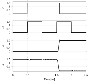
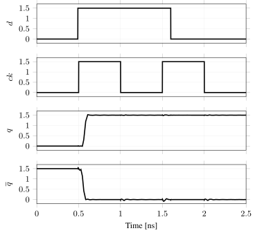
Figure 33: Simulated d, ck, q and qn of the D flip-flop for two setup times, 8 ps and 10 ps. With 8 ps the data changes too close to the rising clock edge at 0.5 ns, the flip-flop does not capture it, and q only goes high at the second edge at 1.5 ns. With 10 ps the data has settled early enough and q rises with the first edge. Two picoseconds separate the two
Left of that boundary the flip-flop still switches, but late: notice how q in the 8 ps plot rises a full clock period after it should. That is the failure mode setup violations produce in a real chip. Nothing is stuck, nothing looks broken on a scope, the data simply arrives one cycle behind, and it only happens on the corners and the temperatures where the launching path is slowest.
Hold time: How long after clk can the data change
Hold time is the same experiment run from the other side. Now the question is not whether the data arrived early enough to be captured, but whether it stayed put long enough afterwards for the capture to finish. Move the data edge towards the clock edge and the flip-flop eventually samples the new value instead of the old one.
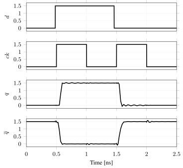
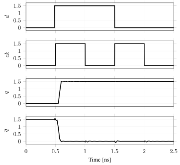
Figure 34: The same signals for two hold times, -40 ps and -30 ps, that is, the data changing 40 ps and 30 ps before the second rising clock edge at 1.5 ns. At -40 ps the flip-flop takes the new low value and q falls. At -30 ps the change is not taken and q stays high for another period
Hold violations are worse than setup violations, and it is worth being clear about why. A setup violation you can fix after the fact by slowing the clock down; the path simply needs more time, and the same silicon works at a lower frequency. A hold violation does not care what the clock frequency is. The data races the clock over a distance that has nothing to do with the period, so a chip that fails hold fails at every frequency, including DC, and the only fix is more silicon: buffers inserted in the fast path, which means another place and route pass.
Timing analysis
Analyze arrival times of all nodes in a combinatorial circuit
\[arrival_i = max_{j \in fanin(i)}{arrival_j} + t_{pd_i} \Rightarrow a_i = max_{j \in fanin(i)}{a_j} + t_{pd_i}\] \[slack_i = required_i - arrival_i\]Positive slack (over PVT2) => Timing is OK Negative slack (over PVT2) => Timing is not OK
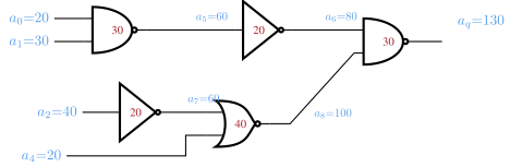
Figure 35: Arrival time propagation through a small combinational circuit, where each gate adds its delay to the largest arrival time at its inputs to give 130 at the output
Timing analysis tools
Commercial Cadence Tempus
Free OpenTimer
What is timing analysis
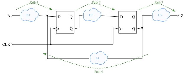
Figure 36: Timing paths through a circuit, each running from a launch point through combinational logic to a capture point, with a table of the four startpoint and endpoint combinations
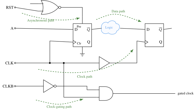
Figure 37: The path types considered in timing analysis - data path, clock path, asynchronous reset path and clock-gating path
What do the tools need?
Input and output delay paths as a function of input transition time and capacitive load, setup and hold time.
cell (INVX1) {
  cell_footprint : inv;
area : 16;
  cell_leakage_power : 0.0221741;
  pin(A)  {
    direction : input;
    capacitance : 0.00932456;
    rise_capacitance : 0.00932196;
    fall_capacitance : 0.00932456;
  }
  pin(Y)  {
    direction : output;
    capacitance : 0;
    rise_capacitance : 0;
    fall_capacitance : 0;
    max_capacitance : 0.503808;
    function : "(!A)";
    timing() {
      related_pin : "A";
      timing_sense : negative_unate;
      cell_fall(delay_template_5x5) {
        index_1 ("0.005, 0.0125, 0.025, 0.075, 0.15");
        index_2 ("0.06, 0.18, 0.42, 0.6, 1.2");
        values ( \
          "0.030906, 0.037434, 0.038584, 0.039088, 0.030318", \
          "0.04464, 0.057551, 0.073142, 0.077841, 0.081003", \
          "0.064368, 0.091076, 0.11557, 0.126352, 0.144944", \
          "0.139135, 0.174422, 0.232659, 0.261317, 0.321043", \
          "0.249412, 0.28434, 0.357694, 0.406534, 0.51187");
      }
      fall_transition(delay_template_5x5) {
        index_1 ("0.005, 0.0125, 0.025, 0.075, 0.15");
        index_2 ("0.06, 0.18, 0.42, 0.6, 1.2");
        values ( \
          "0.032269, 0.0648, 0.087, 0.1032, 0.1476", \
          "0.036025, 0.0726, 0.1044, 0.1236, 0.183", \
          "0.06, 0.0882, 0.1314, 0.1554, 0.2286", \
          "0.1494, 0.1578, 0.2124, 0.2508, 0.3528", \
          "0.288, 0.2892, 0.3192, 0.3576, 0.492");
      }
      cell_rise(delay_template_5x5) {
        index_1 ("0.005, 0.0125, 0.025, 0.075, 0.15");
        index_2 ("0.06, 0.18, 0.42, 0.6, 1.2");
        values ( \
          "0.037639, 0.056898, 0.083401, 0.104927, 0.156652", \
          "0.05258, 0.083003, 0.119028, 0.141927, 0.207952", \
          "0.07402, 0.112622, 0.162437, 0.191122, 0.271755", \
          "0.15767, 0.201007, 0.284096, 0.331746, 0.452958", \
          "0.285016, 0.326868, 0.415086, 0.481337, 0.653064");
      }
      rise_transition(delay_template_5x5) {
        index_1 ("0.005, 0.0125, 0.025, 0.075, 0.15");
        index_2 ("0.06, 0.18, 0.42, 0.6, 1.2");
        values ( \
          "0.031447, 0.059488, 0.0846, 0.0918, 0.138", \
          "0.047167, 0.0786, 0.1044, 0.1224, 0.1734", \
          "0.072, 0.096, 0.1398, 0.1578, 0.222", \
          "0.1866, 0.1914, 0.2358, 0.2748, 0.3696", \
          "0.3648, 0.3648, 0.384, 0.4146, 0.5388");
      }
    }
    internal_power() {
      related_pin : "A";
      fall_power(energy_template_5x5) {
        index_1 ("0.005, 0.0125, 0.025, 0.075, 0.15");
        index_2 ("0.06, 0.18, 0.42, 0.6, 1.2");
        values ( \
          "0.009213, 0.004772, 0.00823, 0.018532, 0.054083", \
          "0.009047, 0.005677, 0.005713, 0.015244, 0.049453", \
          "0.008669, 0.006332, 0.002998, 0.01159, 0.04368", \
          "0.007879, 0.007243, 0.001451, 0.004701, 0.030385", \
          "0.007605, 0.007297, 0.003652, 0.000737, 0.020842");
      }
      rise_power(energy_template_5x5) {
        index_1 ("0.005, 0.0125, 0.025, 0.075, 0.15");
        index_2 ("0.06, 0.18, 0.42, 0.6, 1.2");
        values ( \
          "0.023555, 0.029044, 0.041387, 0.051684, 0.087278", \
          "0.023165, 0.028621, 0.039211, 0.048916, 0.083039", \
          "0.023574, 0.02752, 0.036904, 0.045723, 0.077971", \
          "0.024479, 0.025247, 0.032268, 0.039242, 0.066587", \
          "0.024942, 0.025187, 0.029612, 0.034835, 0.057524");
      }
    }
  }
}
Every gate must be simulated to provide behavior over input transition and load capacitance
All analog blocks must have associated liberty file to describe behavior and timing paths If you integrate analog into digital top flow
Gate Delay
Delay definitions
| Parameter | Name | Description |
|---|---|---|
| t_pdr | max rising propagation delay | input to rising output cross 50 % |
| t_pdf | max falling propagation delay | input to falling output cross 50 % |
| t_pd | propagation delay | t_pd = (t_pdr + t_pdf)/2 |
| t_r | rise time | 20 % to 80 % |
| Parameter | Name | Description |
|---|---|---|
| t_f | fall time | 80 % to 20 % |
| t_cdr | min rising contamination delay | input to rising output cross 50 % |
| t_cdf | min falling contamination delay | input to falling output cross 50 % |
| t_cd | contamination delay | t_cd = (t_cdr + t_cdf)/2 |
Delay estimation
How can we get a reasonably accurate hand calculation model of delay?
\[C \approx 1 \text{ fF}/\mu\text{m}\] \[R \approx 1 \text{ k}\Omega\mu\text{m}\]Inverter with inverter load
\(C \approx 1 \text{ fF}/\mu\text{m}\), \(R \approx 1 \text{ k}\Omega\mu\text{m}\)
\[t_{pd} = R \times 6C = 6RC\] \[t_{pd} = 6 \times 1 \times 10^{3} \times 1 \times 10^{-15} \text{ s}\] \[t_{pd} = 6 \times 10^{-12} = 6 \text{ ps}\]Elmore Delay
\[t_{pd} \approx \sum_{\text{nodes}}{R_{\text{nodes}-to-source} C_i}\] \[= R_1C_1 + (R_1 + R_2)C_2 + ... + (R_1 + R_2 + ... + R_N) C_N\]Good enough for hand calculation
Delay components
Parasitic delay (p)
p = 9 or 12 RC
Independent of load capacitance
Effort delay (f)
f = 5h RC
Proportional to load capacitance
Let’s use process independent unit \(d = \frac{d_{real}}{\tau}\), \(\tau = 3 RC\)
Parasitic delay \(\Rightarrow p = 12 RC / 3 RC = 4\)
Effort delay \(\Rightarrow f = 5h RC / 3RC = \frac{5}{3} h\)
Delay \(\Rightarrow d = f + p = \frac{5}{3}h + 4\)
Logical effort (g) is the ratio of the input capacitance of a gate to the input capacitance of an inverter delivering the same output current
Parasitic delay \(\Rightarrow p = 4\)
Logic effort \(\Rightarrow g = \frac{5}{3}\)
Electrical effort \(\Rightarrow h = 1\)
Effort \(\Rightarrow f = gh\)
Delay \(\Rightarrow d = f + p = gh + p = 5\frac{2}{3}\)
Real delay \(\Rightarrow d = 5\frac{2}{3} \times 3 \text{ ps} = 17 \text{ ps}\)
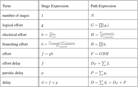
Figure 38: Logical effort summary table giving the stage and path expressions for number of stages, logical effort, electrical effort, branching effort, effort, effort delay, parasitic delay and total delay
Modern IC timing analysis requires computers with advanced programs3
Best number of stages
Which has shortest delay?
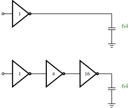
Figure 39: Two ways to drive a load of 64 - a single inverter, and a chain of three inverters sized 1, 4 and 16, with the path effort delay worked out for each
Figure 40: The logical effort table used to evaluate the two candidate paths, giving H equal to 64, G equal to 1, B equal to 1 and path effort F equal to 64
\[H = C_{cout}/C_{in} = 64\] \[G = \prod{g_i} = \prod{1} = 1\] \[B = 1\] \[F = GBH = 64\]One stage, with Sutherland’s classic \(p \approx 1\) per inverter \(f = 64 \Rightarrow D = 64 + 1 = 65\)
Three stage with \(f=4\) \(D_F = 12, p = 3 \Rightarrow D = 12 + 3 = 15\)
The classic textbook numbers above use Sutherland’s parasitic delay of about 1 per inverter; our diffusion-heavy estimate earlier gave $p = 4$. Redo the sums with $p = 4$ and you get 68 against 24 - the absolute numbers move, the conclusion does not: split the path into stages of effort around four.
For close to optimal delay, use \(f = 4\) (Used to be \(f=e\))
Trends
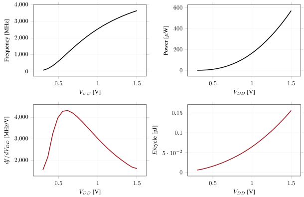
Figure 41: Ring oscillator frequency and power against supply voltage, with the supply sensitivity and the energy per cycle below. The sensitivity peaks near 0.6 V at more than 4 GHz per volt, and the energy per cycle is worst where the ring is fastest
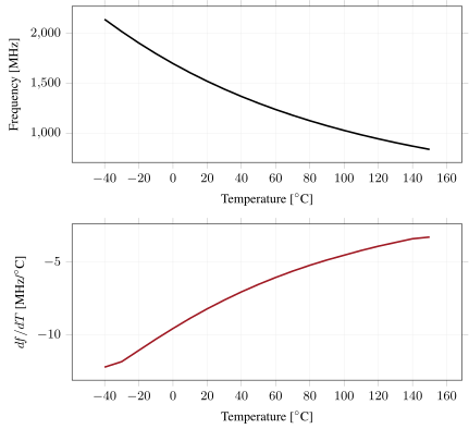
Figure 42: Ring oscillator frequency falling from 2.14 GHz to 0.84 GHz, a factor of 2.6, as temperature rises from minus 40 to 150 degrees Celsius. The slope below runs from about minus 12 MHz per degree in the cold to minus 3 when hot, so the sensitivity is itself temperature dependent
Attack vector
module counter(
               output logic [WIDTH-1:0] out,
               input logic              clk,
               input logic              reset
               );

   parameter WIDTH = 8;

   logic [WIDTH-1:0]                    count;
   always_comb begin
      count = out + 1;
   end

   always_ff @(posedge clk or posedge reset) begin
      if (reset)
        out <= 0;
      else
        out <= count;
   end

endmodule // counter
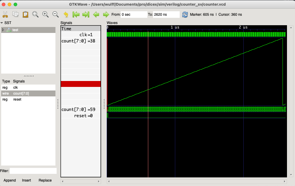
Figure 43: GTKWave view of the 8-bit counter testbench, where the count bus ramps over 2.6 us while clk toggles and reset stays low
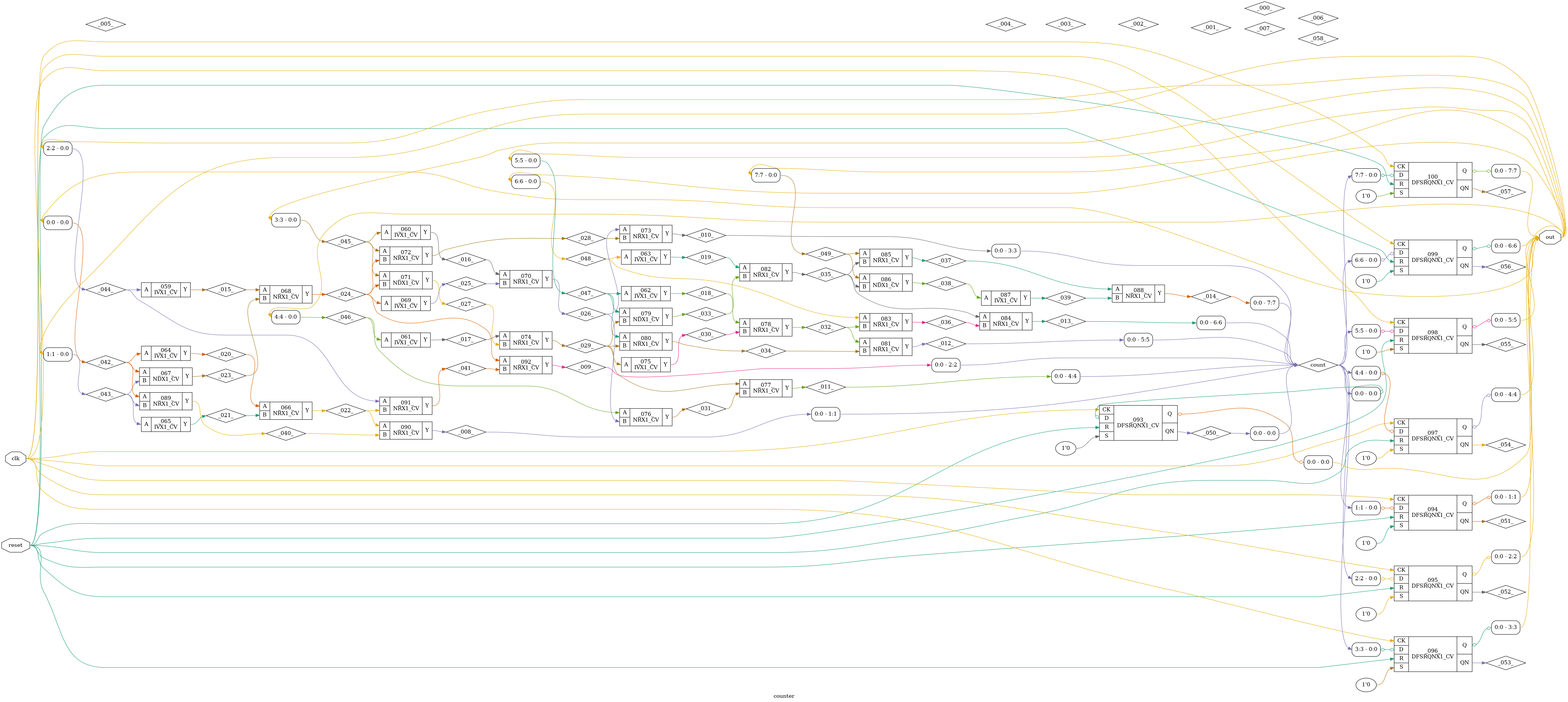
Figure 44: The same 8-bit counter synthesized to the SUN TR GF130N standard cell library, with eight D flip-flops on the right and the increment logic to the left
.SUBCKT counter out_7 out_6 out_5 out_4 out_3 out_2 out_1 out_0 clk reset AVDD AVSS
* SPICE netlist generated by Yosys 0_9 (git sha1 1979e0b1, gcc 10_3_0-1ubuntu1~20_10 -fPIC -Os)
X0 out_2 1 AVDD AVSS IVX1_CV
X1 out_3 2 AVDD AVSS IVX1_CV
X2 out_4 3 AVDD AVSS IVX1_CV
X3 out_5 4 AVDD AVSS IVX1_CV
X4 out_6 5 AVDD AVSS IVX1_CV
X5 out_0 6 AVDD AVSS IVX1_CV
X6 out_1 7 AVDD AVSS IVX1_CV
X7 6 7 8 AVDD AVSS NRX1_CV
X8 out_0 out_1 9 AVDD AVSS NDX1_CV
X9 1 9 10 AVDD AVSS NRX1_CV
X10 10 11 AVDD AVSS IVX1_CV
X11 2 11 12 AVDD AVSS NRX1_CV
X12 out_3 10 13 AVDD AVSS NDX1_CV
X13 out_3 10 14 AVDD AVSS NRX1_CV
X14 12 14 15 AVDD AVSS NRX1_CV
X15 3 13 16 AVDD AVSS NRX1_CV
X16 16 17 AVDD AVSS IVX1_CV
X17 out_4 12 18 AVDD AVSS NRX1_CV
X18 16 18 19 AVDD AVSS NRX1_CV
X19 4 17 20 AVDD AVSS NRX1_CV
X20 out_5 16 21 AVDD AVSS NDX1_CV
X21 out_5 16 22 AVDD AVSS NRX1_CV
X22 20 22 23 AVDD AVSS NRX1_CV
X23 5 21 24 AVDD AVSS NRX1_CV
X24 out_6 20 25 AVDD AVSS NRX1_CV
X25 24 25 26 AVDD AVSS NRX1_CV
X26 out_7 24 27 AVDD AVSS NRX1_CV
X27 out_7 24 28 AVDD AVSS NDX1_CV
X28 28 29 AVDD AVSS IVX1_CV
X29 27 29 30 AVDD AVSS NRX1_CV
X30 out_0 out_1 31 AVDD AVSS NRX1_CV
X31 8 31 32 AVDD AVSS NRX1_CV
X32 out_2 8 33 AVDD AVSS NRX1_CV
X33 10 33 34 AVDD AVSS NRX1_CV
X34 35 clk AVSS reset out_0 35 AVDD AVSS DFSRQNX1_CV
X35 32 clk AVSS reset out_1 36 AVDD AVSS DFSRQNX1_CV
X36 34 clk AVSS reset out_2 37 AVDD AVSS DFSRQNX1_CV
X37 15 clk AVSS reset out_3 38 AVDD AVSS DFSRQNX1_CV
X38 19 clk AVSS reset out_4 39 AVDD AVSS DFSRQNX1_CV
X39 23 clk AVSS reset out_5 40 AVDD AVSS DFSRQNX1_CV
X40 26 clk AVSS reset out_6 41 AVDD AVSS DFSRQNX1_CV
X41 30 clk AVSS reset out_7 42 AVDD AVSS DFSRQNX1_CV
V0 count_0 35 DC 0
V1 43 out_2 DC 0
V2 44 out_3 DC 0
V3 count_3 15 DC 0
V4 45 out_4 DC 0
V5 count_4 19 DC 0
V6 46 out_5 DC 0
V7 count_5 23 DC 0
V8 47 out_6 DC 0
V9 count_6 26 DC 0
V10 48 out_7 DC 0
V11 count_7 30 DC 0
V12 49 out_0 DC 0
V13 50 out_1 DC 0
V14 count_1 32 DC 0
V15 count_2 34 DC 0
.ENDS
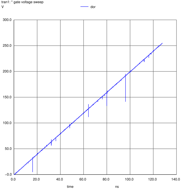
Figure 45: ngspice transient of the reference counter output dor, counting linearly from 0 to 255 over 128 ns
dicex/sim/verilog/counter_sv/counter_attack_tb.cir
VDDA AVDD_ATTACK 0 dc 0.5 pulse(1.5 0.6 tcd trf trf tapw taper)
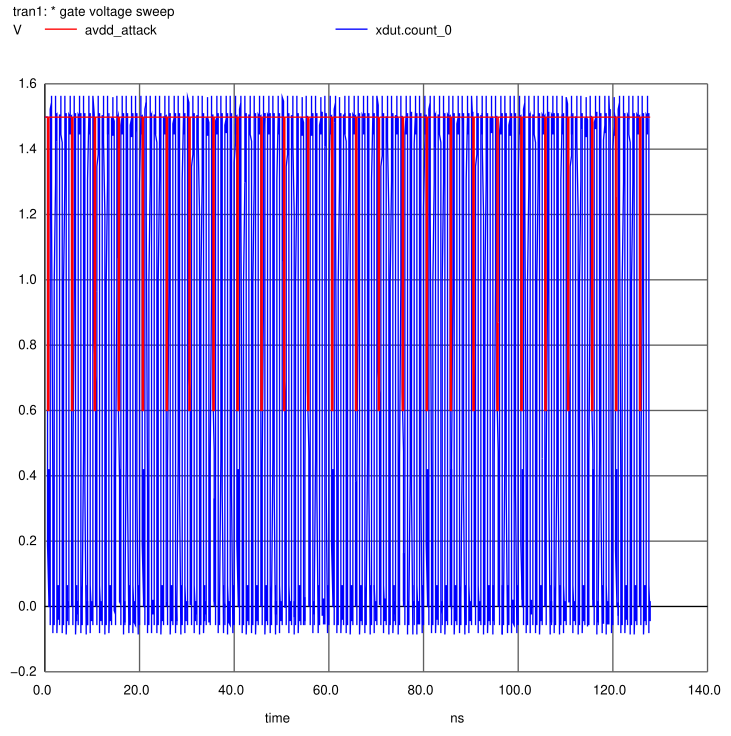
Figure 46: ngspice transient of the attacked supply, pulsed between 1.5 V and 0.6 V, together with the least significant counter bit
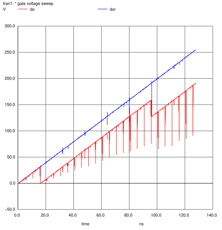
Figure 47: The attacked counter output do in red against the reference output dor in blue, showing the counts lost each time the supply is glitched

Figure 48: The ChipWhisperer web page, an open source platform for side channel power analysis and fault injection attacks on embedded systems
Pick two
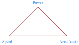
Figure 49: The design trade-off triangle between power, speed and area or cost
Power
What is power?
Instantanious power: \(P(t) = I(t)V(t)\)
Energy : \(\int_0^T{P(t)dt}\) [J]
Average power: \(\frac{1}{T} \int_0^T{P(t)dt}\) [W or J/s]
Power dissipated in a resistor
Ohm’s Law \(V_R = I_R R\)
\[P_R = V_R I_R = I_R^2 R = \frac{V_R^2}{R}\]Charging a capacitor to VDD
Capacitor differential equation \(I_C = C\frac{dV}{dt}\)
\[E_{C} = \int_0^\infty{I_C V_C dt} = \int_0^\infty{ C \frac{dV}{dt} V_C dt} = \int_0^{V_C}{C V dV} = C\left[\frac{V^2}{2}\right]_0^{V_{DD}}\] \[E_{C} = \frac{1}{2} C V_{DD}^2\]Energy to charge a capacitor to a voltage VDD
\[E_{C} = \frac{1}{2} C V_{DD}^2\] \[I_{VDD} = I_C = C \frac{dV}{dt}\] \[E_{VDD} = \int_0^\infty{I_{VDD} V_{DD} dt} = \int_0^\infty{C \frac{dV}{dt} V_{DD} dt} = C V_{DD}\int_0^{V_{DD}}{dV} = C V_{DD}^2\]Only half the energy is stored on the capacitor, the rest is dissipated in the PMOS
Discharging a capacitor to 0
\[E_{C} = \frac{1}{2} C V_{DD}^2\]Voltage is pulled to ground, and the power is dissipated in the NMOS
Power consumption of digital circuits
\[E_{VDD} = C V_{DD}^2\]In a clock distribution network (chain of inverters), every output is charged once per clock cycle
\[P_{VDD} = C V_{DD}^2 f\]Sources of power dissipation in CMOS logic
\[P_{total} = P_{dynamic} + P_{static}\]Dynamic power dissipation
Charging and discharging load capacitances
short-circut current, when PMOS and NMOS conduct at the same time
\[P_{dynamic} = P_{switching} + P_{short circuit}\]Static power dissipation
Subthreshold leakage in OFF transistors
Gate leakage (tunneling current) through gate dielectric
Source/drain reverse bias PN junction leakage
\[P_{static} = \left( I_{sub} + I_{gate} + I_{pn} \right) V_{DD}\]Switching Power in logic gates
Only output node transitions from low to high consume power from \(V_{DD}\)
Define \(P_i\) to be the probability that a node is 1
Define \(\overline{P_i} = 1 - P_i\) to be the probability that a node is 0
Define activity factor (\(\alpha_i\)) as the probability of switching a node from 0 to 1
If the probabilty is uncorrelated from cycle to cycle
\[\alpha_i = \overline{P_i}P_i\]Switching probability
Random data \(P = 0.5\), \(\alpha = 0.25\)
Clocks \(\alpha = 1\)
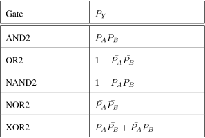
Figure 50: Probability that the output of an AND2, OR2, NAND2, NOR2 or XOR2 gate is 1, expressed in the input probabilities PA and PB
Figure 51: The gate output probability table applied to the network below, where each NAND2 output has probability 3 over 4 of being 1
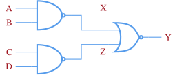
Figure 52: Two NAND2 gates driving a NOR2 gate, giving output probability PY of 1 over 16 and activity factor 15 over 256 when all inputs have probability one half
Assume \(P = P_A = P_B = P_C = P_D = \frac{1}{2}\)
\[P_X = P_Z = 1 - P P = 1 - \frac{1}{4} = \frac{3}{4}\] \[\overline{P_X} = \overline{P_Y} = \frac{1}{4}\] \[P_Y = \frac{1}{4} \times \frac{1}{4} = \frac{1}{16}\] \[\alpha = \frac{1}{16}\left(1 - \frac{1}{16}\right) = \frac{15}{16}\frac{1}{16} = \frac{15}{256}\]
Figure 53: The same gate output probability table, used here alongside the De Morgan simplification of the network
Figure 54: The same NAND-NAND-NOR network, where De Morgan reduces the function to ABCD so that PY is the product of the four input probabilities, 1 over 16
\[\overline{\overline{\text{AB}} + \overline{\text{CD}}}\]Use De Morgan first \(\overline{A+B} = \overline{A} \cdot \overline{B}\)
\[\overline{\overline{\text{AB}} + \overline{\text{CD}}} = \overline{\overline{\text{AB}}} \overline{\overline{\text{CD}}} = ABCD\] \[\Rightarrow P_Y = P_A P_B P_C P_D = \left(\frac{1}{2}\right)^4 = \frac{1}{16}\] \[P_{tot} = \alpha C V_{DD}^2 f\]Strategies to reduce dynamic power
- Stop clock
- Stop activity
- Reduce clock frequency
- Turn off VDD
- Reduce VDD
Figure 55: Synchronous logic drawn as banks of D flip-flops separated by a combinational cloud, the switching activity that costs the dynamic power
Stop clock 4
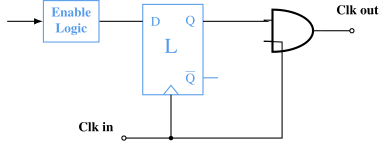
Figure 56: Clock gating, where enable logic feeds a latch and an AND gate so that the output clock only toggles the flip-flops and combinational cloud when the block is enabled
Stop activity
Stopping the clock stops the flip-flops, but it does not necessarily stop the combinational cloud. If the inputs to the cloud keep moving, every gate inside it keeps charging and discharging its load, and the $\alpha C V_{DD}^2 f$ bill arrives whether or not anything downstream cares about the answer. Stopping the activity means breaking the data path into the cloud, so its inputs are held constant and the logic inside simply stops toggling.
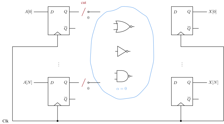
Figure 57: The same flip-flop banks and combinational cloud drawn twice. In the first drawing the cloud is marked at the points where the dynamic power equation can be attacked. In the second the data path from the first flip-flop bank into the cloud is broken, so the cloud sees a constant input and stops switching, while the flip-flops still receive their clock
Reduce frequency
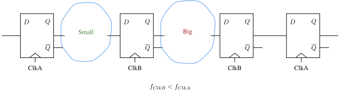
Figure 58: Reducing clock frequency by clocking the big combinational cloud with ClkB and the small cloud with the faster ClkA
Turn off power supply 5
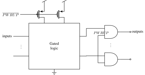
Figure 59: Power gating with PWRUP header switches above the gated logic block and AND gates holding the outputs
Reduce power supply
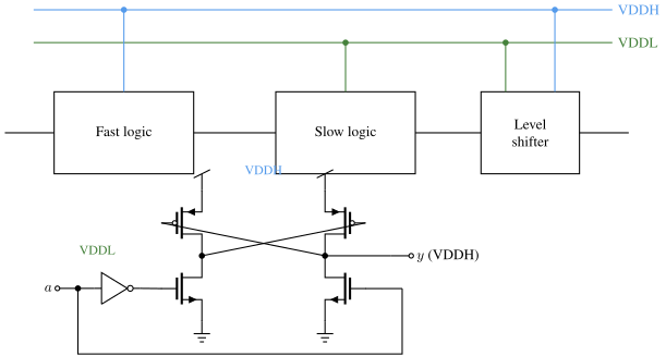
Figure 60: Two supply domains, fast logic on VDDH and slow logic on VDDL, joined by a cross-coupled level shifter
Energy-Delay Product
\[EDP = k\frac{C^2 V_{DD}^3}{(V_{DD}- V_t)^{\text{1 to 2}}}\]Differentiating with respect to \(V_{DD}\) and setting the result to \(0\) it’s possible to work out that
\[V_{DD-opt} = \frac{3}{3-\text{1 to 2}}V_t \in[1.5,3]V_{t}\]Wires
Wire geometry
Pitch = w + s
Aspect ratio (AR) = t/w
These days \(AR \approx 2\)
Metal stack
Often 5 - 10 layers of metal
| Metal | Material | Thickness | Purpose |
|---|---|---|---|
| Metal 1 | Copper | Thin | in gate routing |
| Metal 3 - 5 | Copper | Thicker | Between gates routing |
| RDL | Aluminium | Ultra thick | Can tolerate high forces during wire bonding. |
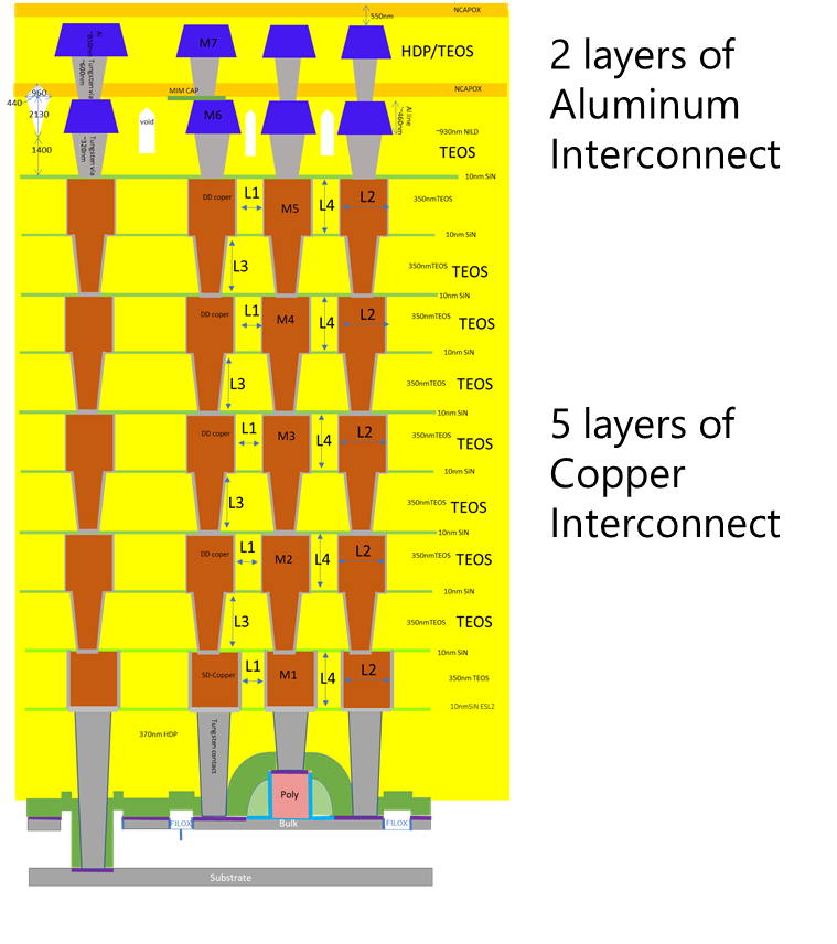
Figure 61: Cross section of the Skywater metal stack, five copper layers M1 to M5 below two aluminium layers M6 and M7
Metal routing rules on IC
Odd numbers metals => Horizontal routing (as far as possible)
Even numbers metals => Vertical routing (as far as possible)
Modeling Interconnect
Resistance narrow size impedes flow
Capacitance through under the leaky pipes
Inductance paddle wheel intertia opposes changes in flow rate
Lumped model
Use 1-segment \(\pi\)-model for Elmore delay
C/2   R   C/2
---/\/\/\---
 |        |
---      ---
---      ---
 |        |
---      ---
 -        -
Wire resistance
\[\text{resistivity} \Rightarrow \rho \text{ [} \Omega\text{m]}\] \[R = \frac{\rho}{t}\frac{l}{w} = R_\square \frac{l}{w}\] \[R_\square = \text{sheet resistance [} \Omega/\square \text{]}\]To find resistance, count the number of squares
\[R = R_\square \times \text{\# of squares}\]Most wires: Copper
\(R_{sheet-m1} \approx \frac{1.7 \mu\Omega cm}{200 nm} \approx 0.1 \Omega/\square\)
\(R_{sheet-m9} \approx \frac{1.7 \mu\Omega cm}{3 \mu m} \approx 0.006 \Omega/\square\)
Pitfalls
Cu atoms diffuse into silicon and can cause damage
Must be surrounded by a diffusion barrier
Difficult high current densities (mA/\(\mu\)m) and high temperature (125 C)
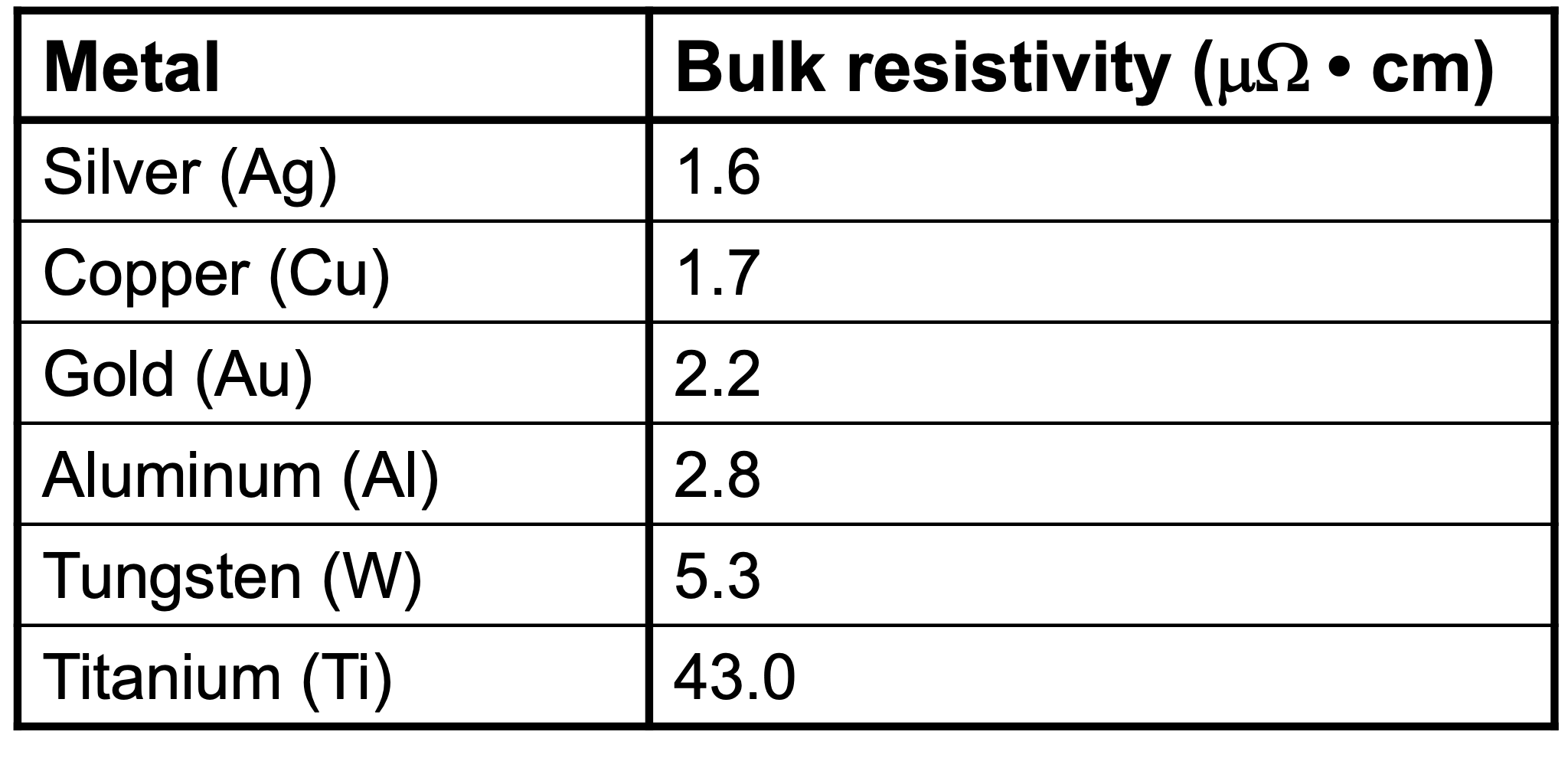
Figure 62: Bulk resistivity in micro-ohm cm for silver, copper, gold, aluminium, tungsten and titanium
Contacts
Contacts and vias can have 2-20 \(\Omega\)
Must use many contacts/vias for high current wires
Wire Capacitance
Dense wires has about \(0.2 \text{ fF/}\mu\text{m}\)
FSM
Mealy machine
An FSM where outputs depend on current state and inputs
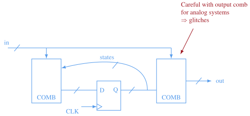
Figure 63: Mealy machine, where the input drives both the next-state logic and the output combinational block, so the output depends on input and current state
Moore machine
An FSM where outputs depend on current state
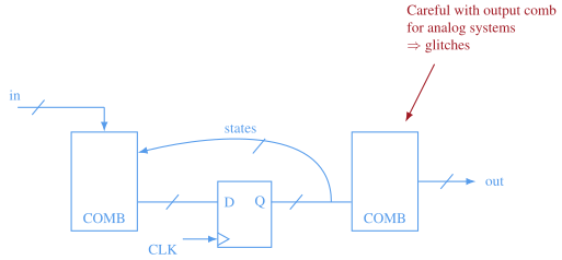
Figure 64: Moore machine, where the output combinational block is driven only by the state register
Mealy versus Moore
| Parameter | Mealy | Moore |
|---|---|---|
| Outputs | depend on input and current state | output depend on current state |
| States | Same, or fewer states than Moore | |
| Inputs | React faster to inputs | Next clock cycle |
| Outputs | Can be asynchronous | Synchronous |
| States | Generally requires fewer states for synthesis | More states than Mealy |
| Counter | A counter is not a mealy machine | A counter is a Moore machine |
| Design | Can be tricky to design | Easy |
dicex/sim/counter_sv/counter.v
module counter(
               output logic [WIDTH-1:0] out,
               input logic              clk,
               input logic              reset
               );
   parameter WIDTH                      = 8;
   logic [WIDTH-1:0]                    count;

   always_comb begin
      count = out + 1;
   end

   always_ff @(posedge clk or posedge reset) begin
      if (reset)
        out <= 0;
      else
        out <= count;
   end

endmodule // counter
Battery charger FSM
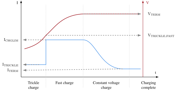
Figure 65: Li-Ion charging profile, charge current and battery voltage against time through trickle charge, fast charge, constant voltage charge and charging complete
Li-Ion batteries
Most Li-Ion batteries can tolerate 1 C during fast charge
For Biltema 18650 cells: \(1\text{ C} = 2950\text{ mA}\) \(0.1\text{ C} = 295\text{ mA}\)
Most Li-Ion need to be charged to a termination voltage of 4.2 V
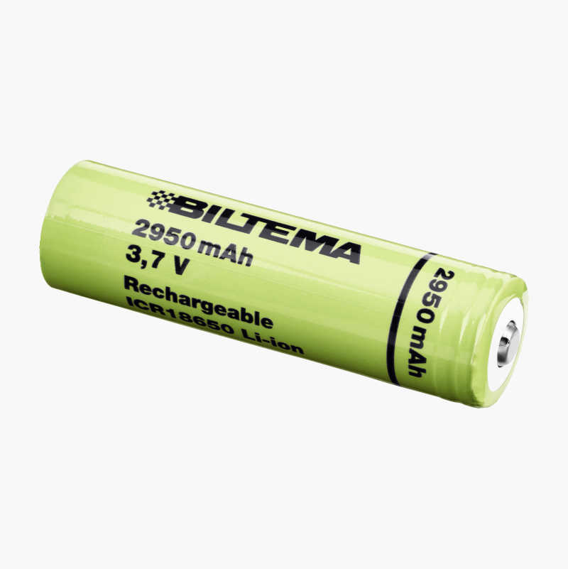
Figure 66: A Biltema ICR18650 rechargeable Li-ion cell rated 2950 mAh at 3.7 V
Too high termination voltage, or too high charging current can cause growth of lithium dendrites, that short + and -. Will end in flames. Always check manufacturer datasheet for charging curves and voltages
Battery charger - Inputs
Voltage above \(V_{TRICKLE}\)
Voltage close to \(V_{TERM}\)
If voltage close to \(V_{TERM}\) and current is close to \(I_{TERM}\), then charging complete
If charging complete, and voltage has dropped (\(V_{RECHARGE}\)), then start again
Figure 67: The charging profile marked with the thresholds the charger senses - the trickle to fast voltage, the termination voltage VTERM and the termination current ITERM
Battery charger - States
Trickle charge (0.1 C)
Fast charge (1 C)
Constant voltage
Charging complete
Figure 68: The charging profile divided into the four charger states - trickle charge at 0.1 C, fast charge at 1 C, constant voltage and charging complete
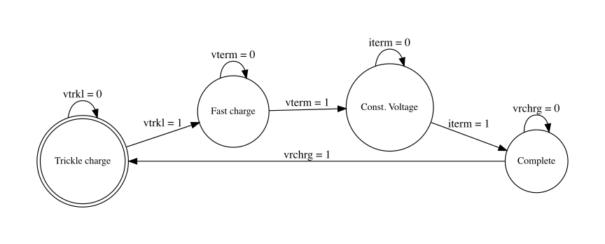
Figure 69: Battery charger state machine, cycling trickle charge, fast charge, constant voltage and complete on the vtrkl, vterm, iterm and vrchrg flags
One way to draw FSMs - Graphviz
digraph finite_state_machine {
    rankdir=LR;
    size="8,5"

    node [shape = doublecircle, label="Trickle charger", fontsize=12] trkl;
    node [shape = circle, label="Fast charge", fontsize=12] fast;
    node [shape = circle, label="Const. Voltage", fontsize=12] vconst;
    node [shape = circle, label="Done", fontsize=12] done;

    trkl -> trkl [label="vtrkl = 0"];
    trkl -> fast [label="vtrkl = 1"];
    fast -> fast [label="vterm = 0"];
    fast -> vconst [label="vterm = 1"];
    vconst-> vconst [label="iterm = 0"];
    vconst-> done [label="iterm = 1"];
    done-> done [label="vrchrg = 0"];
    done-> trkl [label="vrchrg = 1"];

}
dot -Tpdf bcharger.dot -o bcharger.pdf
Figure 70: The battery charger state diagram beside the SystemVerilog case statement that implements the next-state logic
module bcharger( output logic trkl,
        output logic fast,
        output logic vconst,
        output logic done,
        input logic  vtrkl,
        input logic  vterm,
        input logic  iterm,
        input logic  vrchrg,
        input logic  clk,
        input logic  reset
                    );

   parameter TRLK = 0, FAST = 1, VCONST = 2, DONE=3;
   logic [1:0]                   state;
   logic [1:0]                   next_state;

   //- Figure out the next state
   always_comb begin
      case (state)
        TRLK: next_state = vtrkl ? FAST : TRLK;
        FAST: next_state = vterm ? VCONST : FAST;
        VCONST: next_state = iterm ? DONE : VCONST;
        DONE: next_state = vrchrg ? TRLK :DONE;
        default: next_state = TRLK;
      endcase // case (state)
    end
   //- Control output signals
   always_ff @(posedge clk or posedge reset) begin
      if(reset) begin
         state <= TRLK;
         trkl <= 1;
         fast <= 0;
         vconst <= 0;
         done <= 0;
      end
      else begin
         state <= next_state;
         case (state)
           TRLK: begin
              trkl <= 1;
              fast <= 0;
              vconst <= 0;
              done <= 0;
           end
           FAST: begin
              trkl <= 0;
              fast <= 1;
              vconst <= 0;
              done <= 0;

           end
           VCONST: begin
              trkl <= 0;
              fast <= 0;
              vconst <= 1;
              done <= 0;

           end
           DONE: begin
              trkl <= 0;
              fast <= 0;
              vconst <= 0;
              done <= 1;
           end
         endcase // case (state)
      end // else: !if(reset)
   end
endmodule
Synthesize FSM with yosys
dicex/sim/verilog/bcharger_sv/bcharger.ys
# read design
read_verilog -sv bcharger.sv;
hierarchy -top bcharger;

# the high-level stuff
fsm; opt; memory; opt;

# mapping to internal cell library
techmap; opt;
synth;
opt_clean;

# mapping flip-flops
dfflibmap  -liberty ../../../lib/SUN_TR_GF130N.lib

# mapping logic
abc -liberty ../../../lib/SUN_TR_GF130N.lib

# write synth netlist
write_verilog bcharger_netlist.v
read_verilog  ../../../lib/SUN_TR_GF130N_empty.v
write_spice -big_endian -neg AVSS -pos AVDD -top bcharger bcharger_netlist.sp

# write dot so we can make image
show -format dot -prefix bcharger_synth -colors 1 -width -stretch
clean
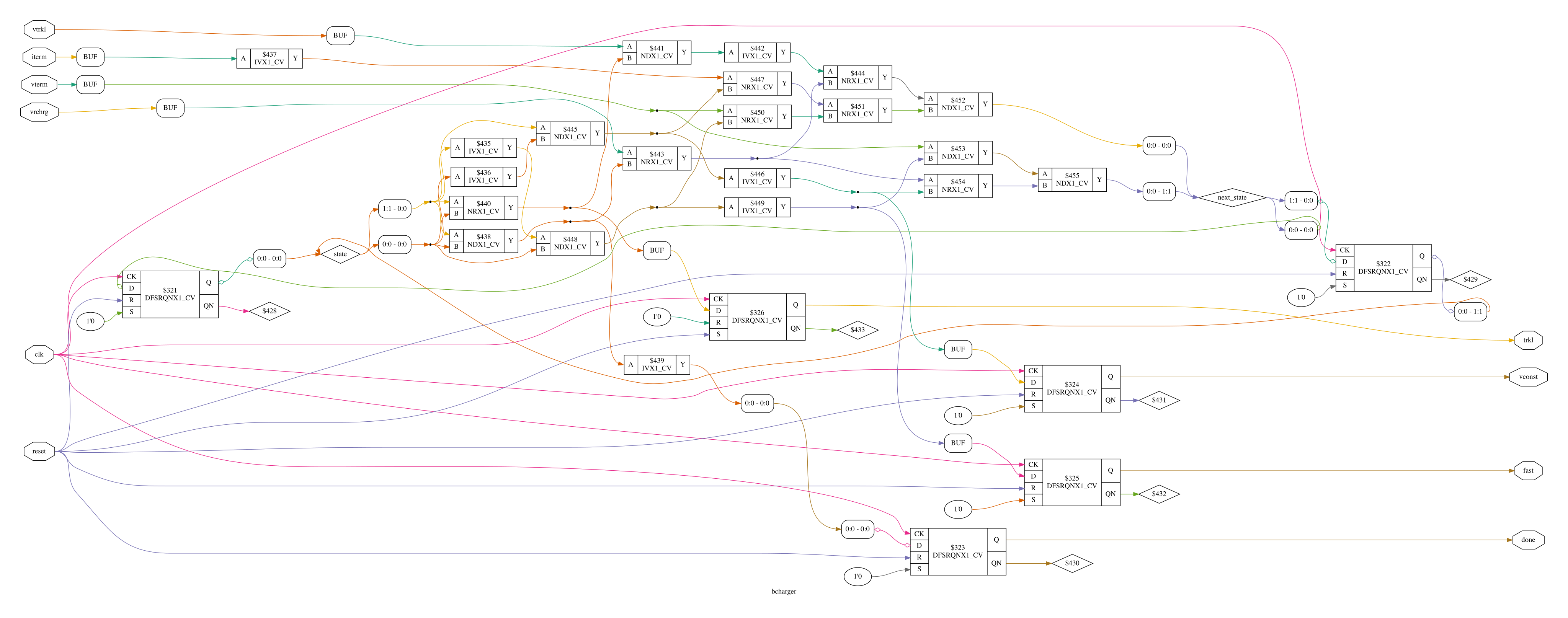
Figure 71: Gate level netlist of the battery charger after yosys synthesis to the SUN TR GF130N cell library, with six flip-flops and the next-state logic between them
Summary
The one-page version of this chapter:
- CMOS logic is a PMOS pull-up network against an NMOS pull-down: the inverter is the atom
- Delay is RC: Elmore for a hand estimate, logical effort for sizing - stage long paths at an effort around four
- Registers, combinational clouds and a clock make synchronous design; setup and hold are checked at every capture
- Static timing analysis walks every path over PVT: positive slack, or it does not ship
- Dynamic power is CV^2 f; leakage is what you pay even when nothing switches
Would you like to know more?
Weste and Harris, CMOS VLSI Design - the standard treatment of logic, timing and power
Sutherland, Sproull and Harris, Logical Effort - the short book that made stage sizing a method rather than a habit
-
Wulff, Carsten and Ytterdal, Trond, A Compiled 9-bit 20-MS/s 3.5-fJ/conv.step SAR ADC in 28-nm FDSOI for Bluetooth Low Energy Receivers 2017 https://doi.org/10.1109/JSSC.2017.2685463 ↩
-
Opportunity for good programmers ↩
-
Often called clock gating ↩
-
Often called power gating ↩