TFE4188 - Lecture 3

Reference and bias

1

Goal for today

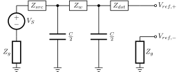
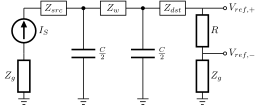
Understand why we need reference and bias circuits

Introduction to circuit architectures

2

Why

3
4
5
6

Bandgap voltage reference

7

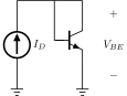
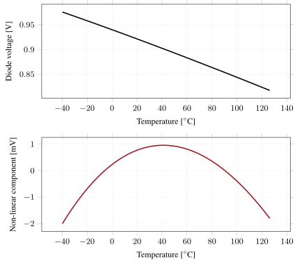
A voltage complementary to temperature (CTAT)

\[I_D = I_S \left(e^{\frac{V_{BE}}{V_T}} - 1\right) + I_B \approx I_S e^{\frac{ V_{BE}}{V_T}}\]

\[V_T = \frac{kT}{q}\]

\[V_{BE} = \frac{k T}{q} \ln{\frac{I_C}{I_S}}\]

\[I_S = q A n_i^2 \left[\frac{D_n}{L_n N_A} + \frac{D_p}{L_p N_D}\right]\]
8

Some algebra (see Diodes)

\(V_{BE} = \frac{kT}{q}(\ell - 3 \ln T) + V_G\)

\[\begin{split} \ell= \ln{I_C} - \ln{qA} - \ln{\left[\frac{D_n}{L_n N_A} + \frac{D_p}{L_p N_D}\right]} \\ - 2 \ln{2} - \frac{3}{2} \ln{m_n^*} - \frac{3}{2}\ln{m_p^*} - 3 \ln{\frac{2 \pi k}{h^2}} \end{split}\]

9
10

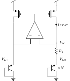
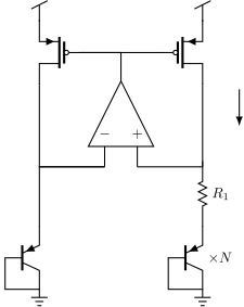
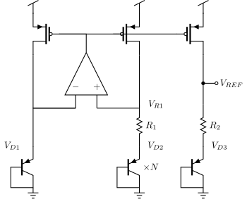
A current proportional to temperature (PTAT)

\[V_{D1} - V_{D2} = V_T \ln{\frac{I_{D}}{I_{S1}}} - V_T \ln{\frac{I_{D}}{I_{S2}}} = V_T \ln{\frac{I_{S2}}{I_{S1}} } = V_T \ln N\]
11

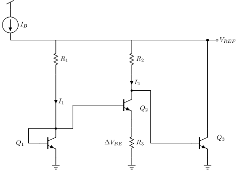
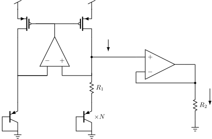
How to combine a CTAT with a PTAT ?

12
13
14

\[\frac{I_1}{I_2} = \frac{R_2}{R_1}\]

\[V_{REF} = V_{BE3} + \frac{R_2}{R_3}\frac{kT}{q}\ln{\frac{R_2}{R_1}}\]
15

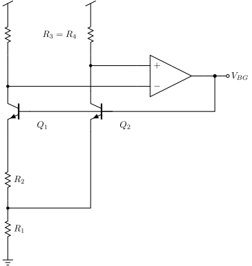
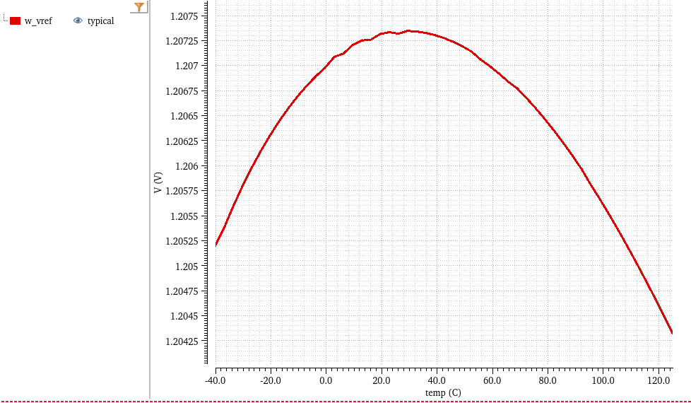
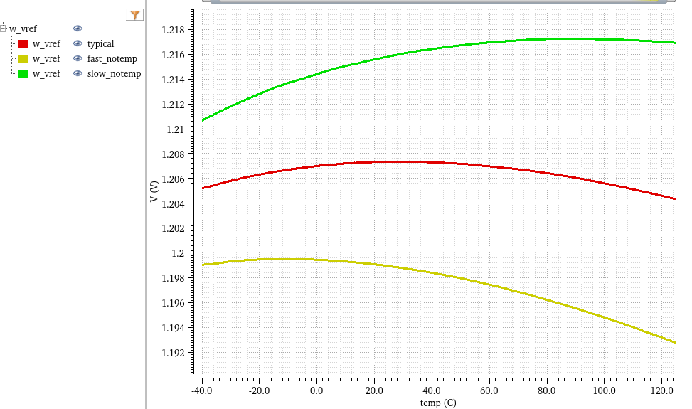
\[V_{BG} = V_{G0} + (m-1)\frac{kT}{q}\ln{\frac{T_0}{T}} +T\left[\frac{k}{q}\ln{\frac{J_2}{J_1}}\frac{2R_1}{R_2} - \frac{V_{G0}- V_{be0}}{T_0}\right]\]
16
17
18

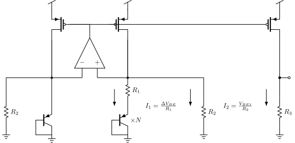
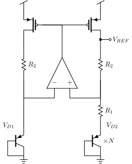
Low voltage bandgap

19
20
21

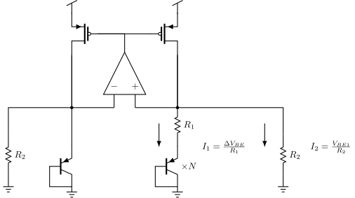
\[I_{PMOS} = \frac{V_D}{R_2} + \frac{\Delta V_D}{R_1}\]
22
23

Curvature correction

24

\[V_{BG} = V_{G0} + (m-1)\frac{kT}{q}\left[1 + \ln{\frac{T_0}{T}}\right]\]

25

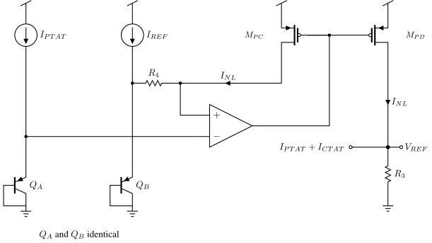
\[V_{BE,A} - V_{BE,B} = \frac{kT}{q}\ln{\frac{I_A}{I_B}}\]

\[V_{BE,A} - V_{BE,B} = \frac{kT}{q}\ln{K} + \frac{kT}{q}\ln{\frac{T}{T_0}}\]

26

\[I_{NL} = \frac{V_{BE,A} - V_{BE,B}}{R_4} = \frac{kT}{qR_4}\left[\ln{K} + \ln{\frac{T}{T_0}}\right]\]

\[V_{REF} = R_3\left[\frac{V_D}{R_2} + \frac{\Delta V_D}{R_1} + I_{NL}\right]\]
27

\[R_4 = \frac{R_2}{m-1}\]

for which \(R_2\) and \(R_4\) must be the same kind of resistor: the ratio only holds over temperature if their temperature coefficients cancel.

28

MOS references

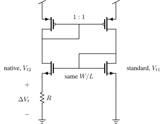
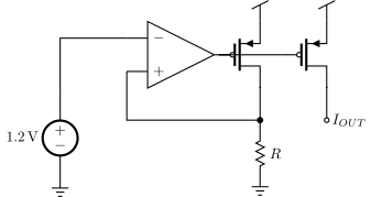
Recognise this one. Do not build it.

29

\[I R = (V_{t1} + V_{eff1}) - (V_{t2} + V_{eff2})\]

\[I = \frac{V_{t1} - V_{t2}}{R} = \frac{\Delta V_t}{R}\]
30

MOS based references that rely on the difference between two threshold voltages are very risky and should not be attempted.

31

The native threshold is set when the ingot is grown

32

FD-SOI moves the problem, it does not remove it

33

The back gate is a trimming knob, not a reference

34

Bias

Sometimes we just need a current

35

Voltage to current conversion

36

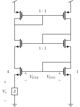
GM Cell

\[V_o = V_{GS1} - V_{GS2} = V_{eff1} + V_{tn} - V_{eff2} - V_{tn} = V_{eff1} - V_{eff2}\]

\[\frac{1}{2} \mu_n C_{ox} \frac{W_1}{L_1} V_{eff1}^2 = \frac{1}{2} \mu_n C_{ox} 4 \frac{W_1}{L_1} V_{eff2}^2\]

\[V_{eff1} = 2 V_{eff2}\]

\[g_{m} = \frac{2 I_d}{V_{eff}}\]

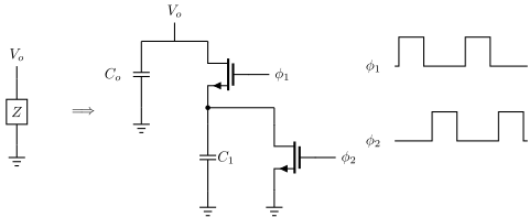
\[I = \frac{ V_{eff1}}{2Z}\]

so the impedance sets the transconductance directly

\[g_{m1} = \frac{1}{Z}\]
37
38

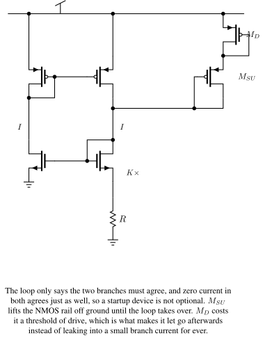
Every one of these loops can fail to start

39
40

Summary

  • A reference must not move with supply, temperature or process; a bias must track what its circuit needs
  • V_BE falls with temperature (CTAT), the difference of two V_BE at a density ratio rises (PTAT, V_T ln N): weight and add for a flat bandgap near 1.2 V
  • Widlar and Brokaw are the classic ways to force the PTAT current and do the sum
  • Distribute currents, not voltages: a routed V_B collects every IR drop on the die
  • The constant-gm loop sets gm = 1/R for everything it biases
  • Every self-biased loop is equally happy at zero current - the startup branch is not optional, and it must let go afterwards
41

Would you like to know more?

New developments in IC voltage regulators [@widlar71]

A simple three-terminal IC bandgap reference [@brokaw74]

A CMOS bandgap reference circuit with sub-1-V operation [@banba99]

A sub-1-V 15-ppm//spl deg/C CMOS bandgap voltage reference without requiring low threshold voltage device [@leung02]

The Bandgap Reference [@razavi16]

The Design of a Low-Voltage Bandgap Reference [@razavi21]

42

Thanks!

43