OTAs

1

The headroom budget

\[V_{DD} = 0.8 \text{ V}, V_{t} \approx 0.4\text{ V}\]

One gate-source voltage

\[V_{GS} \approx 0.5 \text{ V}\]

One saturated current source, one cascode

\[V_{DSAT} \approx 0.1 \text{ V each}\]

Stack of two gate-source voltages? Dead.

Telescopic cascode with swing? Dead.

2

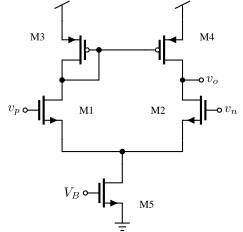
Five transistor OTA

\[A = g_{m1} (r_{ds2} \parallel r_{ds4})\]

\[\omega_{ugf} = \frac{g_{m1}}{C_L}\]

Output swing: \(V_{DD} - 2 V_{DSAT}\)
3

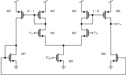
Current mirror OTA

\[A = K g_{m1} (r_{ds6} \parallel r_{ds8})\]

\[\omega_{ugf} = \frac{K g_{m1}}{C_L}\]

Slew rate: \(\pm K I_{tail} / C_L\)
4

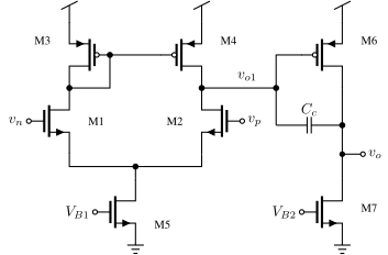
Two stage (Miller) OTA

\[A = g_{m1}(r_{ds2} \parallel r_{ds4}) \times g_{m6}(r_{ds6} \parallel r_{ds7})\]

\[\omega_{ugf} = \frac{g_{m1}}{C_c}\]

Pole splitting: dominant pole down, output pole out to \(\approx \frac{g_{m6}}{C_L}\)
5

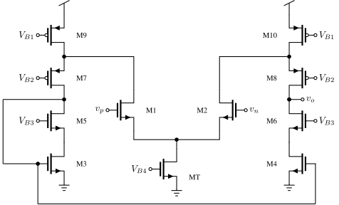
Folded cascode

\[A \approx g_{m1} \left( g_{m8} r_{ds8} (r_{ds10} \parallel r_{ds2}) \, \parallel \, g_{m6} r_{ds6} r_{ds4} \right)\]

\[\omega_{ugf} = \frac{g_{m1}}{C_L}\]

Output swing: \(V_{DD} - 4 V_{DSAT}\)
6

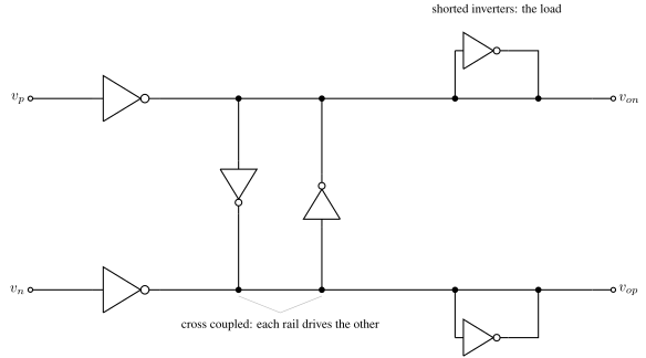
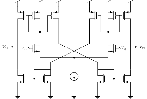
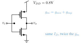
Inverter based OTAs

7
8

Bulk driven input

Bulk as signal input

\[g_{s} \approx (n-1) g_m \approx 0.2 g_m\]

Input common mode: rail to rail

Cost: five times less transconductance, and the bulk-source diode must stay off

9

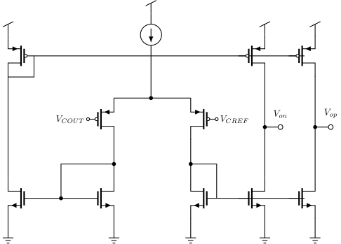
Fully differential

10

Common mode feedback

11

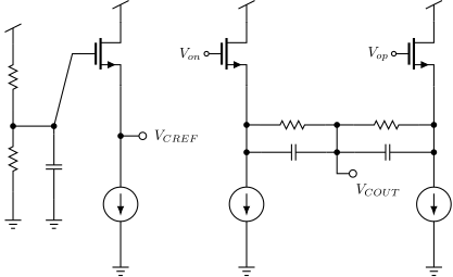
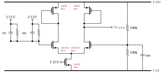
Sensing the common mode

12

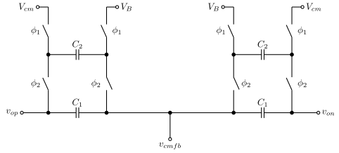
Switched capacitor CMFB

13

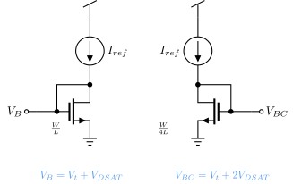
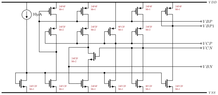
Bias circuits

14

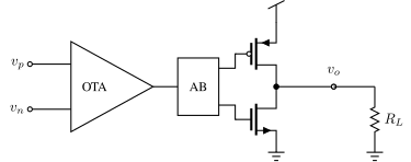
From OTA to op amp

15

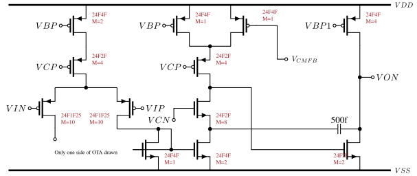
A complete OTA, sized

16
17
18

Dynamic amplifiers

Dynamic gain

\[A \approx \frac{g_m T}{C}\]

Power

\[P \propto C V_{DD}^2 f_s\]

Only in sampled systems, and everywhere in modern ADCs

19

Choosing

Topology Gain Swing Best at
Five transistor \(g_m r_{ds}\) good buffers, bias loops
Current mirror \(K g_m r_{ds}\) good drive, SC circuits
Two stage Miller \((g_m r_{ds})^2\) best gain + swing
Folded cascode \(g_m (g_m r_{ds}^2)\) poor SC settling
Inverter based \(g_m r_{ds}\) good sub-1V, low power
Dynamic \(g_m T/C\) - ADCs
20

Verifying the OTA

Analysis Testbench Look for
Operating point closed loop, DC every device saturated, all corners
Loop gain stb / broken loop DC gain, UGF, phase margin > 60 deg
CMFB loop gain stb on the CM loop stable on its own, faster than the disturbance
Noise AC noise, closed loop input referred, thermal and flicker
Offset Monte Carlo mismatch sigma of input referred offset
Swing sweep output, plot gain where the gain collapses
Slew and settling large signal step settles to accuracy in the time budget
PSRR / CMRR AC from supply / CM worst case versus frequency
Start-up transient from zero bias and CMFB wake up, always
Power DC, all corners the budget holds where it is slowest
21

Summary

  • At 0.8 V: never stack two gate-source voltages, and count every saturation voltage
  • Five transistor OTA first; upgrade only for a reason
  • Need drive: current mirror OTA. Need gain: two stage. Need one-stage gain: folded cascode
  • Miller compensation splits the poles; the unity gain frequency is gm over Cc; mind the RHP zero
  • Inverters amplify: both transconductances for one branch current, and Nauta's OTA needs no tail
  • Fully differential doubles swing but must pay the CMFB tax
  • In sampled systems, dynamic amplifiers win the power argument
22

Would you like to know more?

23