


Who
Carsten Wulff
Why
Example of a temperature sensor
How it works
One way to make a temperature sensor is to create a temperature dependent oscillator, and then measure the frequency of the oscillator. In Figure 0 we can see an overview.
A bandgap circuit is used to make a current that is proportional to absolute temperature ($I_{PTAT}$) and a voltage that is complementary to absolute temperature ($V_{CTAT}$). A relaxation oscillator converts the current and voltage into a frequency ($f_{OSC}$). A digital finite-state-machine and a counter converts the frequency to a digital value that is proportional to temperature.

Figure 0: System overview
This temperature sensor was made to conform to the specification at The Project: Design a temperature sensor.
For more information on the oscillator, see Schematics.
To measure the frequency of the oscillator we need a frequency reference. One reference that is usually available in a MCU system is a 32768 Hz oscillator ($f_{32KI}$ in Figure 0). The reason for that specific frequency is to accurately be able to count to 1 second with a binary counter, and apparently to have a frequency for the crystal that is higher than 20 kHz, so we can’t hear it (according to https://youtu.be/_2By2ane2I4?si=8ltUNqAPL71zCQUW).
The principle of operation of the FSM and counter can be seen in Figure 1.
The FSM starts in an IDLE state where a counter is reset. Next the temperature dependent oscillator is started, and a number of oscillator pulses are counted. The FSM runs on LF_CLK and we use the count x LF_CLK to measure the oscillation frequency.
After one clock period the FSM powers down the oscillator. In the CAPTURE state the value of the counter is stored, and the FSM returns to idle.
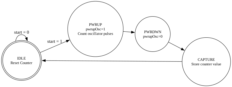
Figure 1: Finite-State Machine to control temperature sensor
A waveform of the sequence can be seen in Figure 2. When the signal start is asserted the FSM transitions to power up the oscillator (pwrupOsc=1), and we can notice the clkOsc counts the clock pulses of the oscillator. On the next lfClk the oscillator is shut down and the counter naturally stops. The value from the oscillator is stored in the cycles register.
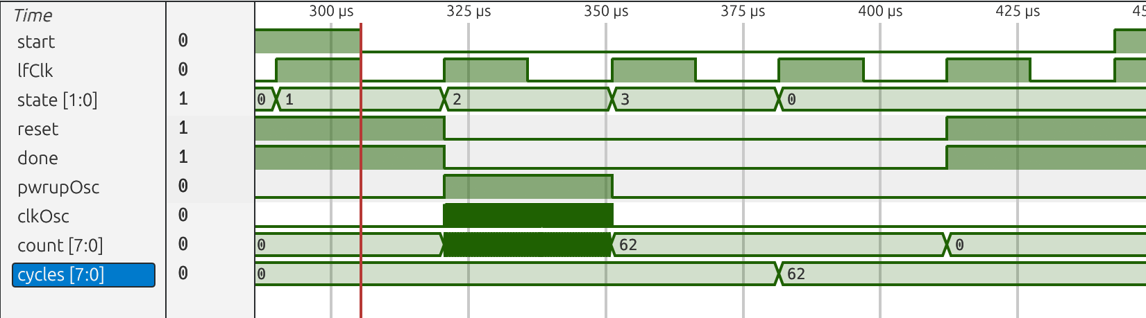
Figure 2: Waves from simulation of the oscillator
In the testbench I store the cycles, and the testbench temperature to a file, and use tb.py to plot the transfer function.
I use a physical model of the oscillator (LELO_TEMP.py) to create a function to turn the frequency back to a temperature. It can be seen that the frequency has a non-zero second order derivative, and thus, the shape of the curve needs to be compensated for. See the python model for details.
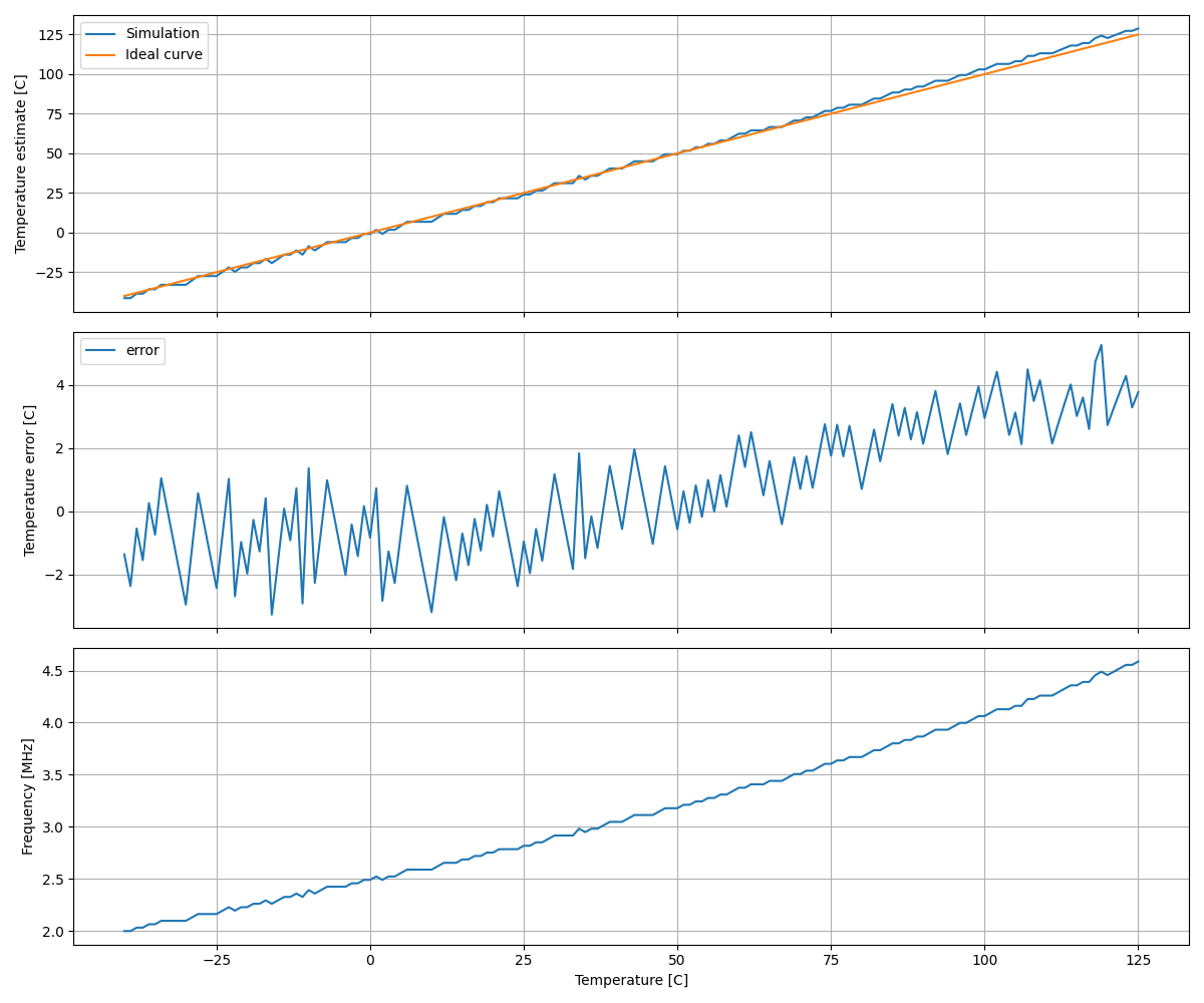
Figure 3: Simulation of the verilog model of the oscillator
| What | Cell/Name |
|---|---|
| Schematic | design/LELO_TEMP_SKY130A/LELO_TEMP.sch |
| Layout | design/LELO_TEMP_SKY130A/LELO_TEMP.mag |
| Verilog Model | design/LELO_TEMP_SKY130A/LELO_TEMP.v |
| Verilog Counter | rtl/tempCounter.v |
| Verilog Fsm | rtl/tempFsm.v |
| Verilog TB | sim/tb_lelo_temp/tb.v |
| Analog top TB | sim/LELO_TEMP/tran.spi |
How to test
Power the tile, then drive PWRUP_ANA (ui[0]) high to power the analog core up. The temperature-dependent oscillator output appears on OSC_TEMP (uo[0]); measure its frequency with a counter or a logic analyzer. The frequency tracks temperature. Sweep the ambient and record frequency versus temperature to calibrate. Drive PWRUP_ANA low and the core powers down to leakage.
No external hardware is required beyond something that can measure frequency.
Signal interface
| Signal | Direction | Domain | Description |
|---|---|---|---|
| VDD_1V8 | Input | VDD_1V8 | Main supply |
| PWRUP_1V8 | Input | VDD_1V8 | Power up the temperature dependent oscillator |
| OSC_TEMP_1V8 | Output | VDD_1V8 | Temperature dependent frequency |
| VSS | Input | Ground |
Key parameters
| Parameter | Min | Typ | Max | Unit |
|---|---|---|---|---|
| Technology | Skywater 130 nm | |||
| AVDD | 1.7 | 1.8 | 1.9 | V |
| Temperature | -40 | 27 | 125 | C |
| Oscillation frequency | 1.1 | 2.0 | 4.0 | MHz |
| Supply current (25 C) | 63 | 83 | 107 | uA |
| Power-down current (25 C) | 10 | 11 | 50 | nA |
| Temperature error, 1-point cal. | -6.7 | +9.1 | C | |
| Temperature error, 2-point cal. | -7.3 | +5.3 | C |
Measured on the extracted view over the full industrial temperature range (-40 to 125 C): Typ is typical process at 1.8 V and 27 C (the typical frequency runs 1.4 to 3.2 MHz over that range); Min/Max span the extreme test condition corners (process corners at 1.7 to 1.9 V). Over the commercial range (0 to 70 C) the temperature error is -3.7..+2.9 C (1-point) and -1.9..+1.5 C (2-point).
Simulation graphs
All result figures show both views: Sch is the schematic netlist, Lay the parasitic extraction of the finished layout. In the error figures the left column is one-point calibration, the right column two-point; the dashed red lines are the industrial spec (-40 to 125 C, ±15 C / ±10 C), the dotted box the commercial spec (0 to 70 C, ±10 C / ±5 C), and each panel prints its worst positive and negative error.
The oscillator frequency itself shifts down about 20 % from Sch to Lay under the extracted parasitics – the calibration absorbs most of it, which is the point of calibrating:
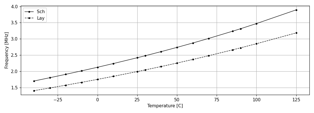
Figure 4: Oscillator frequency versus temperature, typical
Typical temperature error of the sensor is low. The frequency-to-
temperature model is calibrated per netlist view (the effective
oscillator capacitance is fitted from the typical run – see
LELO_TEMP.FIT in py/LELO_TEMP.py), so both views
show only the real residual curvature, about ±1 C after one-point
calibration:
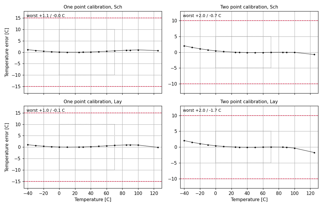
Figure 5: Temperature error, typical
Over the extreme test condition corners (ETC) and mismatch the temperature error increases:
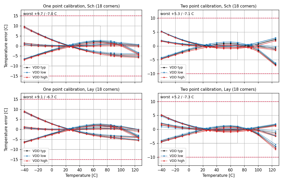
Figure 6: Temperature error, extreme test conditions (PVT)
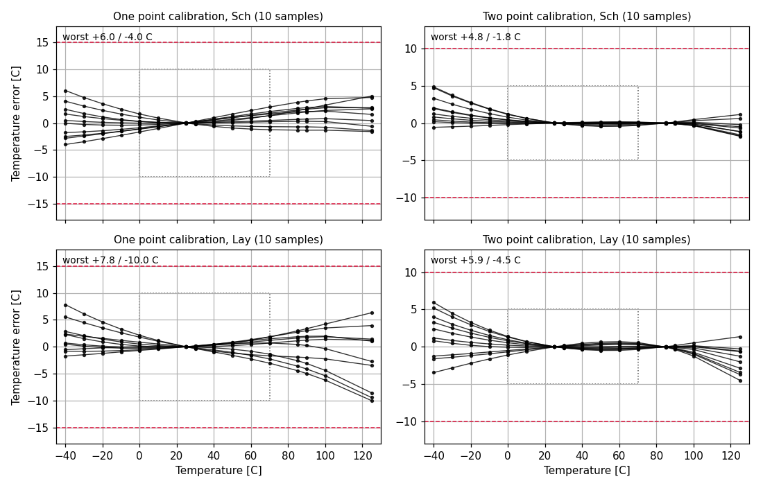
Figure 7: Temperature error, mismatch (10 samples)
The full result tables with spec checking are in sim/LELO_TEMP/README.md.