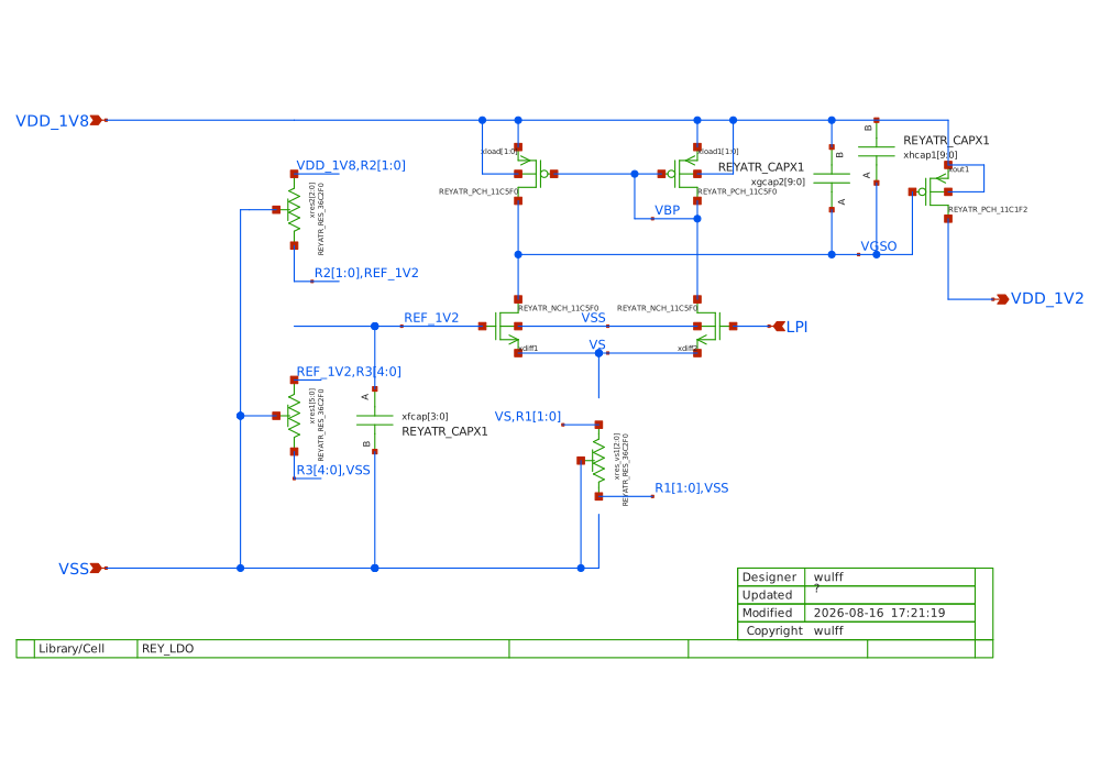
Schematics
- REY_LDO_SKY130A
- Reference
- Amplifier and pass device
- Feedback
- Measured (schematic, sim/REY_LDO, 2026-08-16)
REY_LDO_SKY130A
REY_LDO
A 1.2 V low-dropout regulator, deliberately minimal: no bandgap, no bias input, no enable. Everything is referred to the supply and to the sheet resistance of the poly ladder.
Reference
The reference is a nine-unit resistor ladder (REYATR_RES_36C2F0) from VDD_1V8 to VSS, tapped three units from the top:
\[V_{REF} = \frac{6}{9} \cdot AVDD = \frac{2}{3} \cdot 1.8 = 1.2 V\]The tap is filtered to VSS by four MIM units. Because the reference is ratiometric in the supply, the output is too: this LDO does not reject its supply, it divides it. A 100 mV line step moves the output by ~67 mV, and the small-signal PSRR is
\[PSRR = 20 \log_{10}{\frac{2}{3}} \approx -3.5 dB\]at any frequency the loop can follow. That is the design’s own floor; real rejection needs a supply-independent reference in front of LPI.
Amplifier and pass device
The error amplifier is an NMOS pair (REF_1V2 against the feedback input LPI) with a PMOS mirror load. There is no tail current source: the tail is a three-unit resistor ladder to VSS, so the bias is set by the same sheet resistance as the reference,
\[I_{tail} = \frac{V_S}{3 R_u} \approx \frac{0.45}{39 k} \approx 11 uA\]with $R_u \approx 13 k\Omega$ (two res_high_po stripes of 20.4
squares in series). The mirror’s output drives VGSO, the gate of a
common-source PMOS pass device (L=0.22, the only short-channel
device in the cell). Twenty MIM units sit from VGSO to VDD_1V8.
The divider draws $1.8 / 9 R_u \approx 15 uA$, so the quiescent current is dominated by the resistors:
| Branch | Current |
|---|---|
| Reference divider | ~15 uA |
| Tail + mirror | ~11 uA |
| Total measured | 16–33 uA over corners |
Feedback
The loop closes OUTSIDE the cell: LPI must be tied to VDD_1V2 (or to a divider on it, for a higher output). Unity feedback gives 1.2 V out.
Measured (schematic, sim/REY_LDO, 2026-08-16)
| Parameter | Li (no load) | Lh (200 uA) |
|---|---|---|
| DC loop gain | 63 dB | 63 dB |
| Unity gain freq | 39 MHz | 162 MHz |
| Phase margin | -1° | 24° |
| PSRR (flat) | -2.4 dB | -2.4 dB |
The loop is not stable. The compensation caps from VGSO to VDD_1V8 make a pole at the gate but no Miller path across the pass device, so the gate pole and the output pole sit too close together and the phase is gone before the gain is. The transient testbench shows sustained ringing at light load, and the operating point itself lands anywhere between 1.08 and 1.20 V run to run because the solver settles mid-oscillation. Compensation must be reworked (Miller cap from VGSO to VDD_1V2, or a real output capacitor) before this block is used.
The testbenches (loop stability with a Tian probe, 0 to 200 uA load
step, -100 mV line step, PSRR over frequency) live in
sim/REY_LDO, all runnable across
corners with make all.