l9_amplifiers
- TFE4152 - Lecture 9
- Current mirrors and Amplifiers
- Goal for today
- Process variations - Correction
- \(I \ne i\)
- \(V \ne v\)
- \(I = I_{bias} + i\)
- \(V = V_{bias} + v\)
- Current Mirror
- Current mirror \(r_{in}\)
- Current mirror \(r_{out}\)
- Source degeneration
- Source degeneration \(r_{out}\)
- Cascode current mirror
- One more current mirror …
- Source follower
- Source follower - Gain
- Source follower - \(r_{out}\)
- Common gate
- Common gate - \(r_{in}\)
- Common gate - \(r_{out}\)
- Common gate - \(r_{out}\)
- Common gate - Gain
- Common gate - Gain
- Common gate - Gain
- Common source
- Common source - Gain
- Differential pair
- Diff pairs are cool
TFE4152 - Lecture 9
Current mirrors and Amplifiers
Source
| Week | Book | Monday | Book | Friday |
|---|---|---|---|---|
| 34 | Introduction, what are we going to do in this course. Why do you need it? | WH 1 , WH 15 | Manufacturing of integrated circuits | |
| 35 | CJM 1.1 | pn Junctions | CJM 1.2 WH 1.3, 2.1-2.4 | Mosfet transistors |
| 36 | CJM 1.2 WH 1.3, 2.1-2.4 | Mosfet transistors | CJM 1.3 - 1.6 | Modeling and passive devices |
| 37 | Guest Lecture - Sony | CJM 3.1, 3.5, 3.6 | Current mirrors | |
| 38 | CJM 3.2, 3.3,3.4 3.7 | Amplifiers | CJM, CJM 2 WH 1.5 | SPICE simulation and layout |
| 39 | Verilog | Verilog | ||
| 40 | WH 1.4 WH 2.5 | CMOS Logic | WH 3 | Speed |
| 41 | WH 4 | Power | WH 5 | Wires |
| 42 | WH 6 | Scaling Reliability and Variability | WH 8 | Gates |
| 43 | WH 9 | Sequencing | WH 10 | Datapaths - Adders |
| 44 | WH 10 | Datapaths - Multipliers, Counters | WH 11 | Memories |
| 45 | WH 12 | Packaging | WH 14 | Test |
| 46 | Guest lecture - Nordic Semiconductor | |||
| 47 | CJM | Recap of CJM | WH | Recap of WH |
Goal for today
Current mirrors
Amplifiers
Errata
Process variations - Correction
Wrong Assume strong inversion and active \(V_{eff} = \sqrt{2\mu_p C_{ox} \frac{W}{L} I_1}\)
Correct Assume strong inversion and active \(V_{eff} = \sqrt{\frac{2}{\mu_p C_{ox} \frac{W}{L}} I_1}\)
Large signal vs small signal
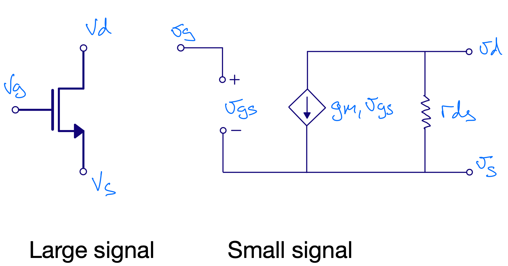
\(I \ne i\)
\(V \ne v\)
\(I = I_{bias} + i\)
\(V = V_{bias} + v\)


Current Mirror
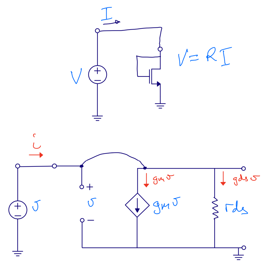
\(M_1\) is diode connected (\(V_G = V_D\))
Current mirror \(r_{in}\)
\[r_{ds} = \frac{1}{g_{ds}}\] \[r_{in} = \frac{v}{i}\] \[i = g_m v + g_{ds} v\] \[r_{in} = \frac{1}{gm + gds} \approx \frac{1}{gm}\]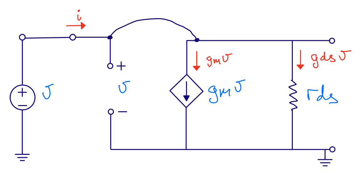
Current mirror \(r_{out}\)
Output voltage does not affect \(v_{gs}\)
\[r_{out} = r_{ds}\]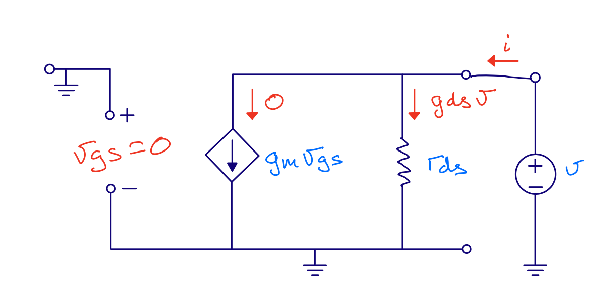
Source degeneration
What is the operating region of M3 and M4?
What is the operating region of M1 and M2?
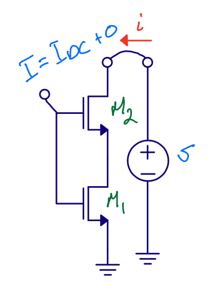

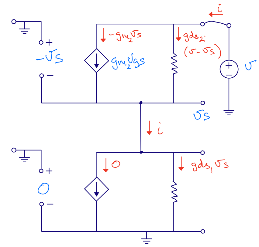

Source degeneration \(r_{out}\)
\[v_{gs1} = 0\] \[v_{gs2} = -v_s\] \[i = g_{ds1} v_s \Rightarrow v_s = i r_{ds1}\] \[r_{out} = \frac{v}{i}\] \[i = -g_{m2} v_{s} + \frac{v - v_s}{r_{ds2}}\]
\(i = -g_{m2} v_{s} + \frac{v - v_s}{r_{ds2}}\) insert \(v_s = i r_{ds1}\)
\[i = -i g_{m2} r_{ds1} + \frac{v - i r_{ds1}}{r_{ds2}}\] \[i r_{ds2} + i g_{m2}r_{ds1}r_{ds2} + i r_{ds1} = v\] \[r_{ds2} + g_{m2}r_{ds1}r_{ds2} + r_{ds1} = \frac{v}{i}\] \[r_{out} = r_{ds2} \left[1 + r_{ds1} \left( \frac{1}{r_{ds2}} + g_{m2}\right )\right]\] \[r_{out} = r_{ds2}\left[1 + r_{ds1}(g_{m2} + g_{ds2})\right]\]
Cascode current mirror
Same equation as source degeneration, but \(M_2\) is in saturation
\[r_{ds2(\text{saturation})} > r_{ds2(\text{linear})}\] \[r_{out} = r_{ds4}[1 + r_{ds2}(g_{m4} + g_{ds2})]\]One more current mirror …
“High speed, high gain OTA in a digital 90nm CMOS technology” Berntsen, Wulff, Ytterdal
image ../ip/berntsen.png removed
Amplifiers
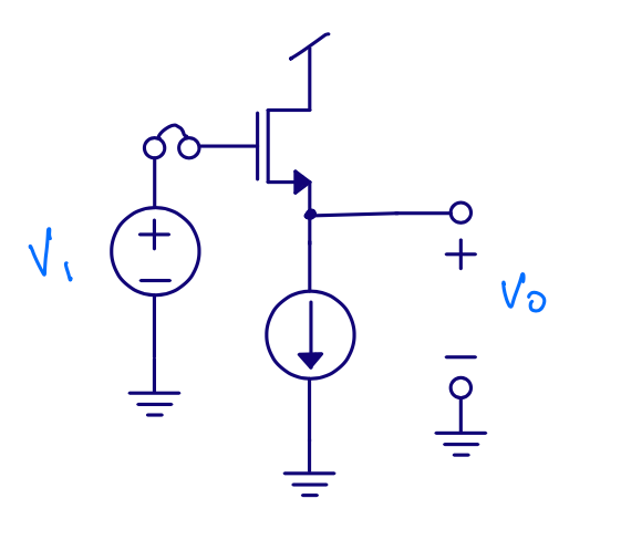
Source follower
Source follower
Input resistance \(\approx \infty\)
Gain \(A = \frac{v_o}{v_i}\)?
Output resistance \(r_{out}\)?

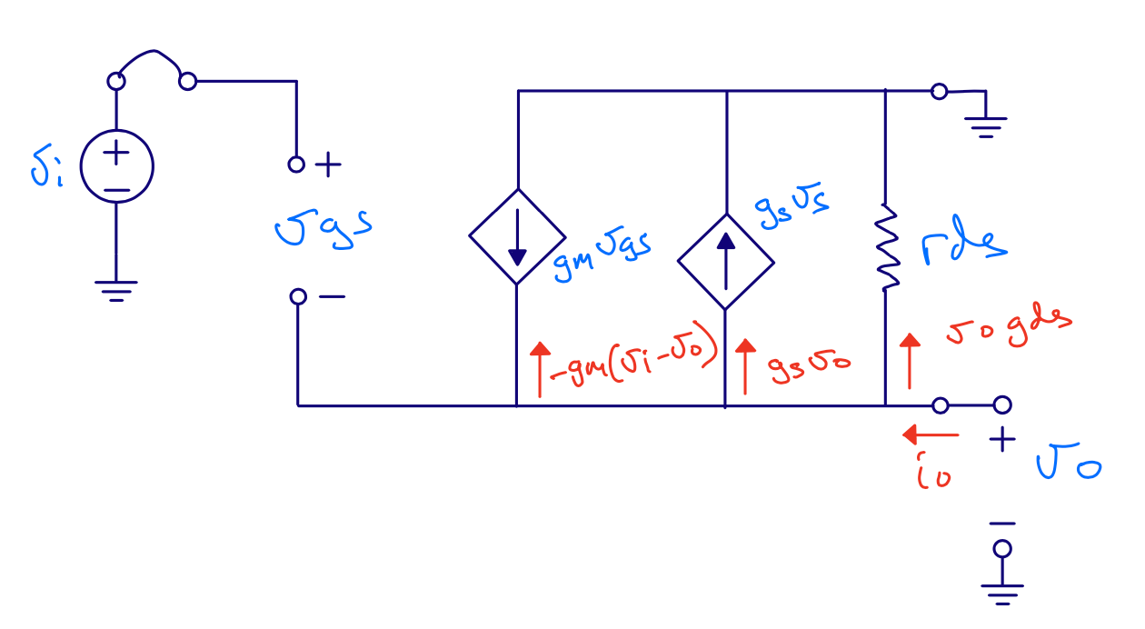
Source follower - Gain
\[i_o = v_o (g_{ds} + g_{s}) - g_{m} v_i + v_o g_m\] \[i_o = 0\] \[g_m v_i = v_o ( g_m + g_s + g_{ds} )\] \[A = \frac{v_o}{v_i} = \frac{g_m}{g_m + g_{ds} + g_s}\]Gain is less than 1

Source follower - \(r_{out}\)
\[i_o = v_o (g_{ds} + g_{s}) - g_{m} v_i + v_o g_m\] \[v_i = 0\] \[i_o = v_o (g_{ds} + g_{s} + g_m)\] \[r_{out} = \frac{v_o}{i_o} = \frac{1}{g_m + g_{ds} + g_{s}}\] \[r_{out} \approx \frac{1}{g_m}\]
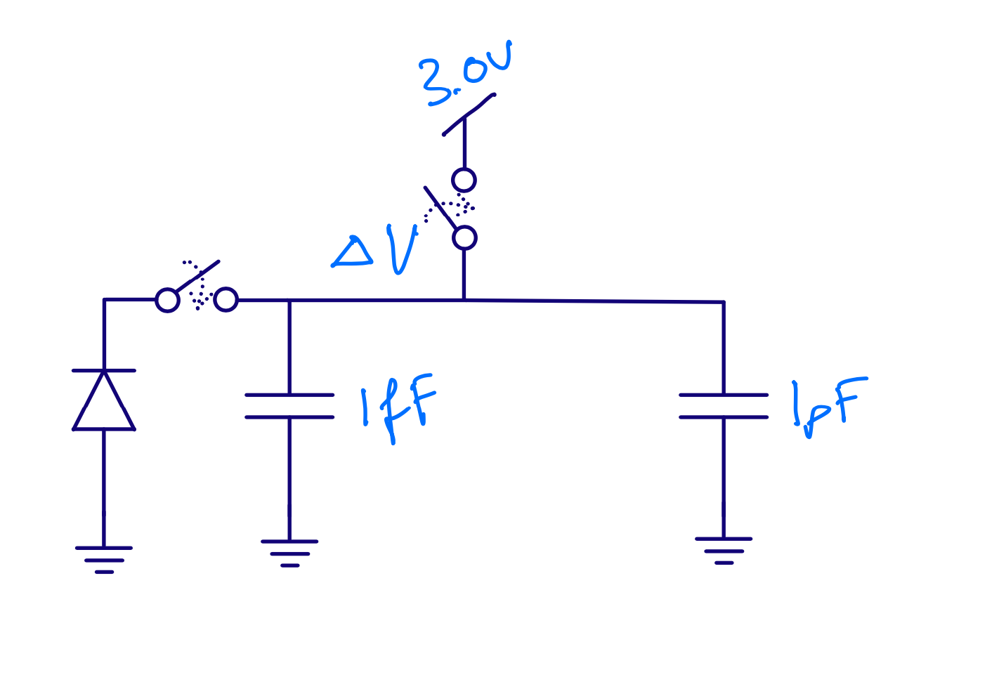
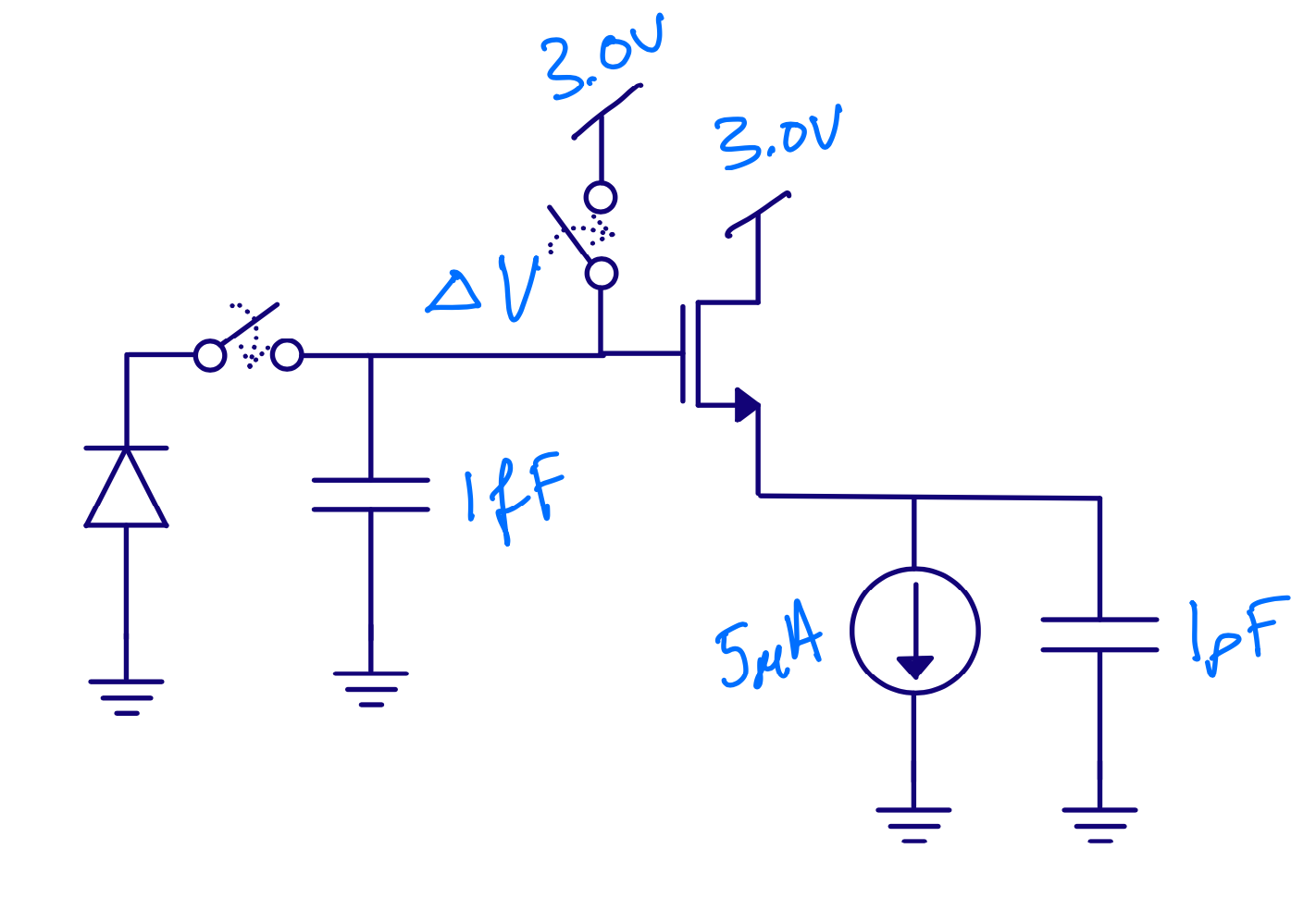
Assume 100 electrons
\[\Delta V = Q/C = -1.6 \times 10^{-19} \times 100 / (1\times 10^{-15}) = - 16\text{ mV}\]

Common gate
Common gate
Input resistance ?
Gain ?
Output resistance ?
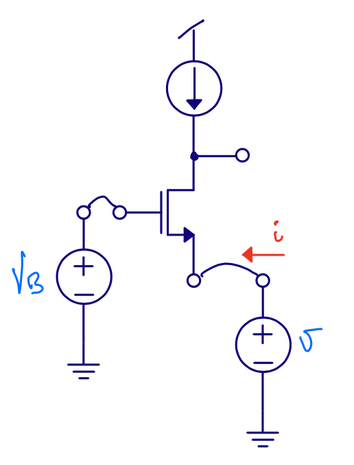

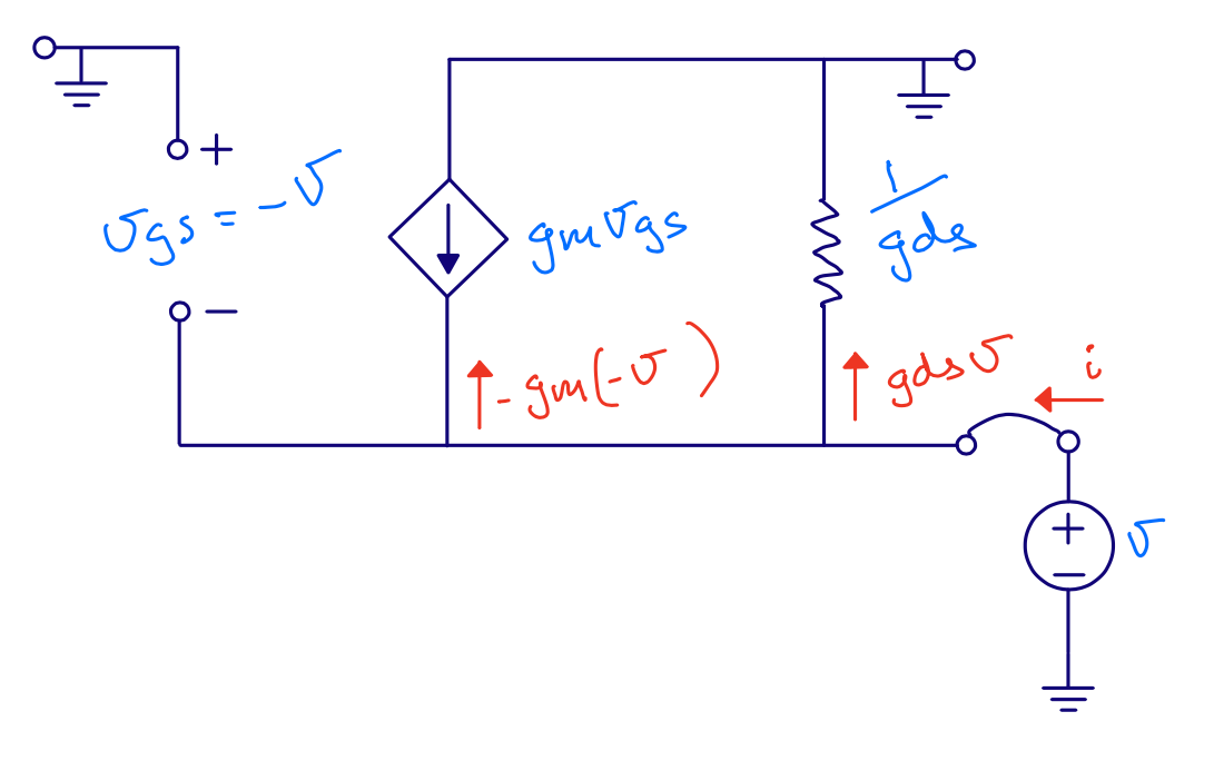
Common gate - \(r_{in}\)
\[i = g_m v + g_{ds} v\] \[r_{in} = \frac{1}{g_m + g_{ds}} \approx \frac{1}{g_m}\]However, we’ve ignored load resistance.
\[r_{in} \approx \frac{1}{g_m}\left(1 + \frac{R_L}{r_{ds}}\right)\]
Common gate - \(r_{out}\)
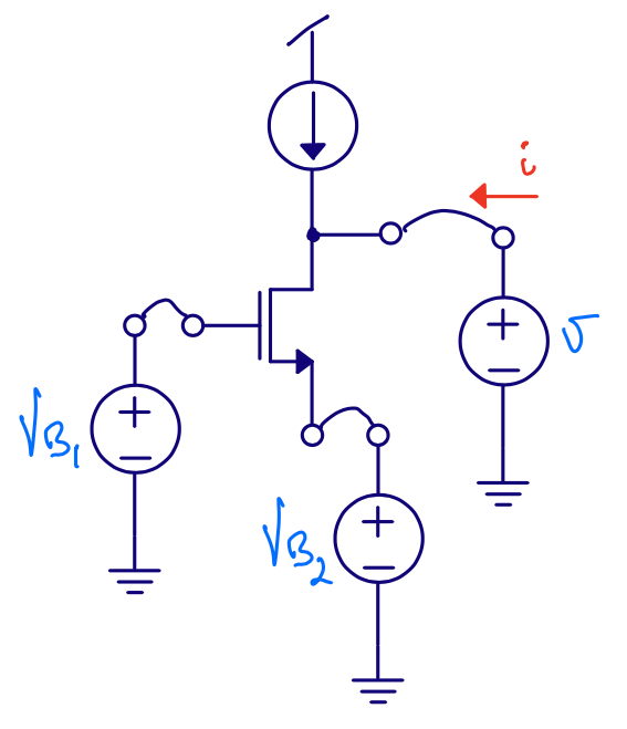

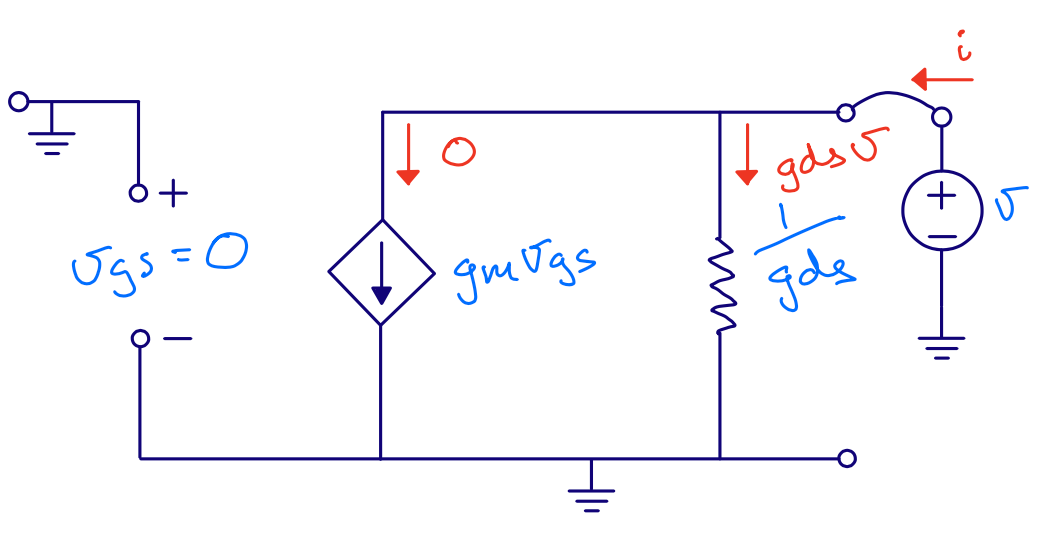
Common gate - \(r_{out}\)
\[r_{out} = r_{ds}\]
Common gate - Gain
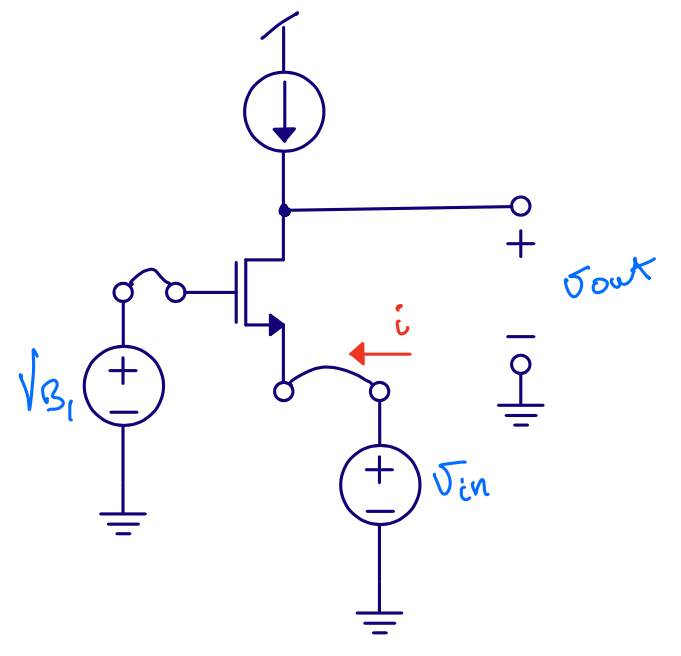

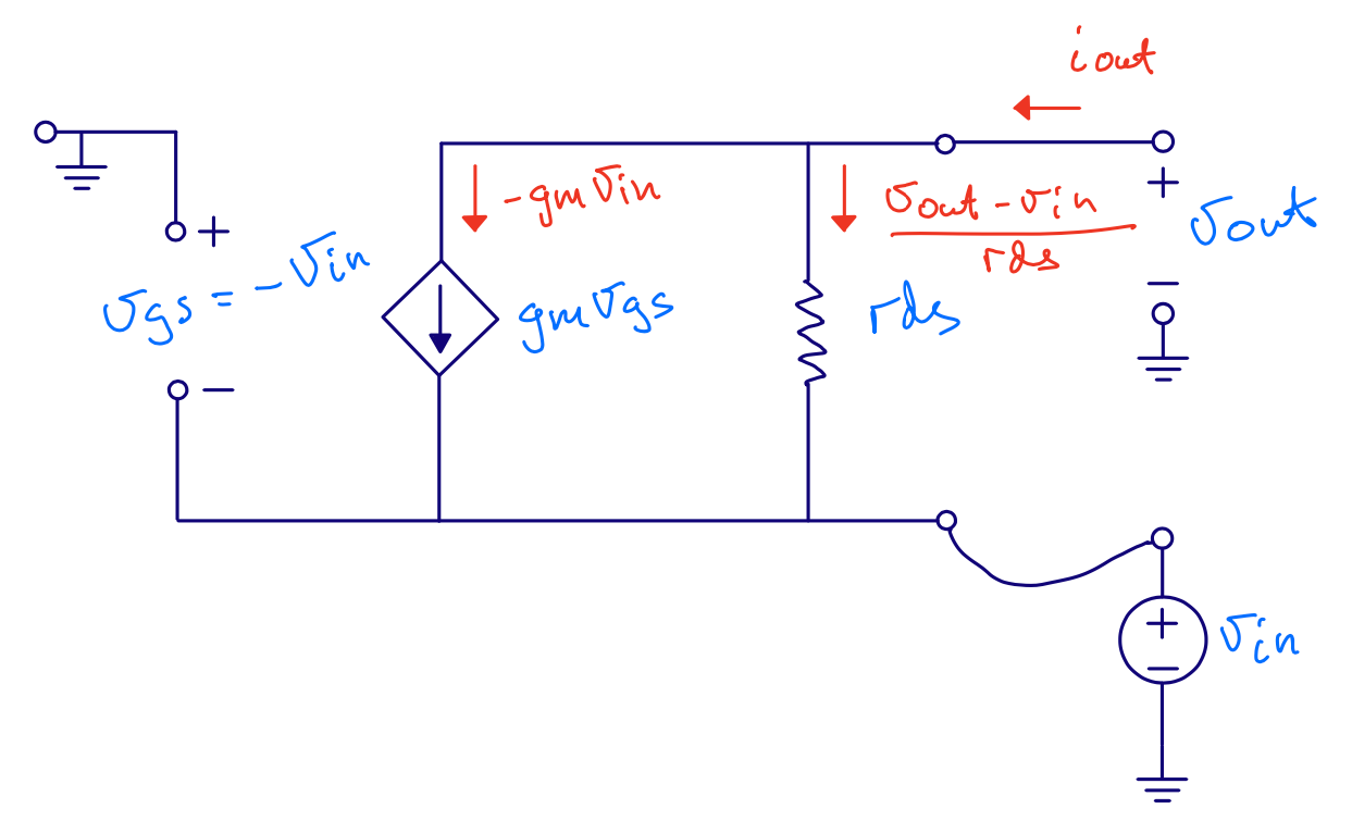
Common gate - Gain
\[i_{o} = - g_m v_{i} + \frac{v_{o} - v_{i}}{r_{ds}}\] \[i_{o} = 0\] \[0 = - g_m v_{i} r_{ds} + v_{o} - v_{i}\] \[v_{i} (1 + g_m r_{ds}) = v_{o}\] \[\frac{v_o}{v_i} = 1 + g_m r_{ds}\]
Common gate - Gain
We’ve ignored bulk effect (\(g_s\)), source resistance (\(R_S\)) and load resistance (\(R_L\))
\[A = \frac{(g_{m} + g_s + g_{ds})(R_L||r_{ds})}{1 + R_S\left(\frac{g_m + g_s + g_{ds}}{1 + R_L/r_{ds}}\right)}\]If \(R_L >> r_{ds}\), \(R_S = 0\) and \(g_s = 0\)
\[A = \frac{(g_{m} + g_{ds})r_{ds}}{1} = 1+ g_m r_{ds}\]
Common source
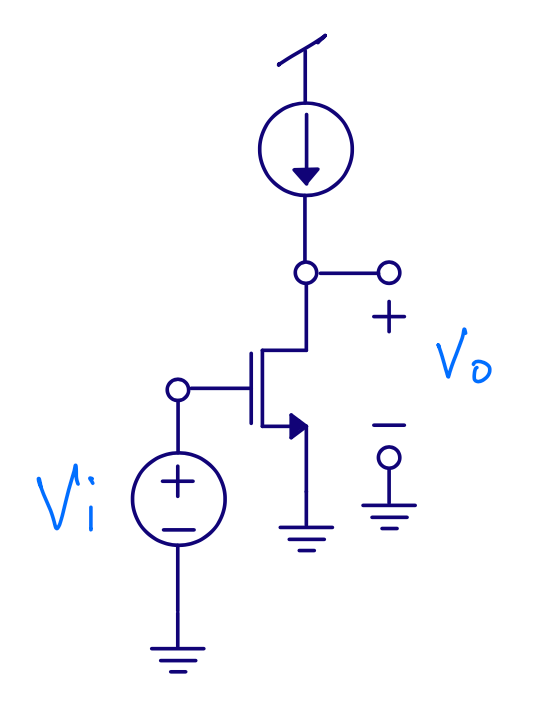
Common source
Input resistance \(r_{in} \approx \infty\)
Output resistance \(r_{out} = r_{ds}\), it’s same circuit as the output of a current mirror
Gain ?

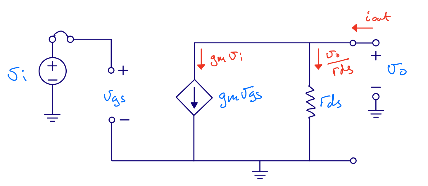
Common source - Gain
\[i_{o} = g_m v_i + \frac{v_o}{r_{ds}}\] \[i_o = 0\] \[-g_m v_i = \frac{v_o}{r_{ds}}\] \[\frac{v_o}{v_i} = - g_m r_{ds}\]
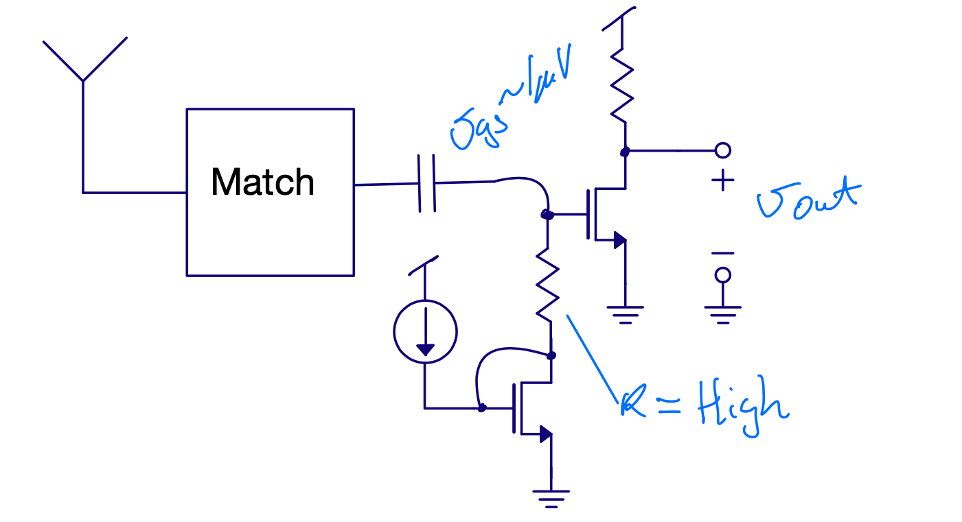
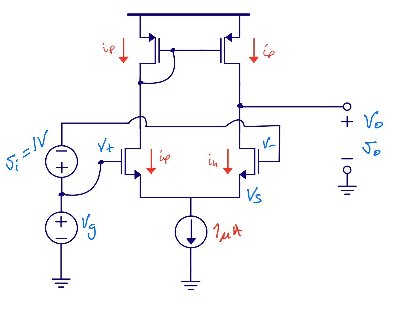
Differential pair
Input resistance \(r_{in} \approx \infty\)
Gain \(A = g_m r_{ds}\)
Output resistance \(r_{out} = r_{ds}\)
Best analyzed with T model of transistor (see CJM page 31)
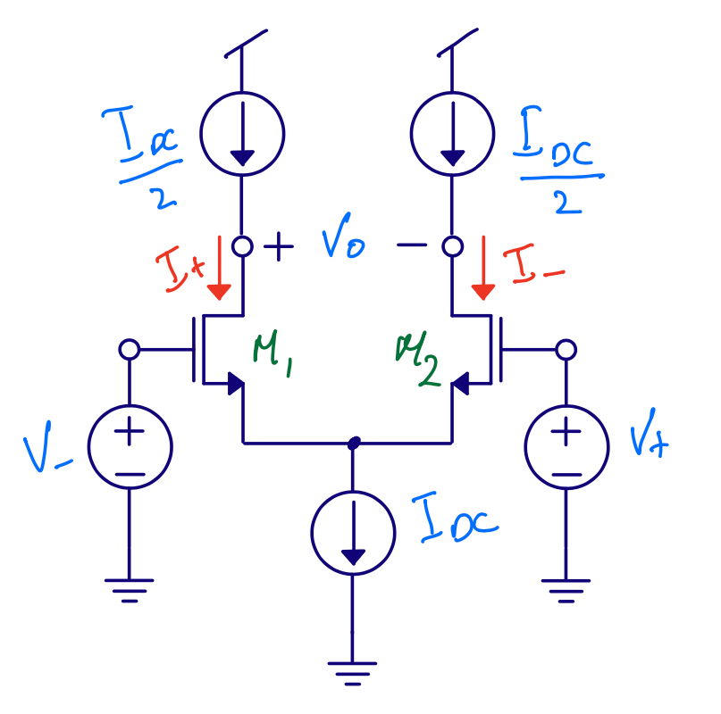
Diff pairs are cool

Can choose between
\[v_o = g_m r_{ds} v_i\]and
\[v_o = -g_m r_{ds} v_i\]by flipping input (or output) connections
