| Week | Book | Monday | Book | Friday |
|---|---|---|---|---|
| 34 | Introduction, what are we going to do in this course. Why do you need it? | WH 1 , WH 15 | Manufacturing of integrated circuits | |
| 35 | CJM 1.1 | pn Junctions | CJM 1.2 WH 1.3, 2.1-2.4 | Mosfet transistors |
| 36 | CJM 1.2 WH 1.3, 2.1-2.4 | Mosfet transistors | CJM 1.3 - 1.6 | Modeling and passive devices |
| 37 | Guest Lecture - Sony | CJM 3.1, 3.5, 3.6 | Current mirrors | |
| 38 | CJM 3.2, 3.3,3.4 3.7 | Amplifiers | CJM, CJM 2 WH 1.5 | SPICE simulation and layout |
| 39 | Verilog | Verilog | ||
| 40 | WH 1.4 WH 2.5 | CMOS Logic | WH 3 | Speed |
| 41 | WH 4 | Power | WH 5 | Wires |
| 42 | WH 6 | Scaling Reliability and Variability | WH 8 | Gates |
| 43 | WH 9 | Sequencing | WH 10 | Datapaths - Adders |
| 44 | WH 10 | Datapaths - Multipliers, Counters | WH 11 | Memories |
| 45 | WH 12 | Packaging | WH 14 | Test |
| 46 | Guest lecture - Nordic Semiconductor | |||
| 47 | CJM | Recap of CJM | WH | Recap of WH |
| ## Goal for today |
| Current mirrors |
| Amplifiers |
Wrong Assume strong inversion and active $$ V_{eff} = \sqrt{2\mu_p C_{ox} \frac{W}{L} I_1} $$
Correct Assume strong inversion and active $$ V_{eff} = \sqrt{\frac{2}{\mu_p C_{ox} \frac{W}{L}} I_1} $$

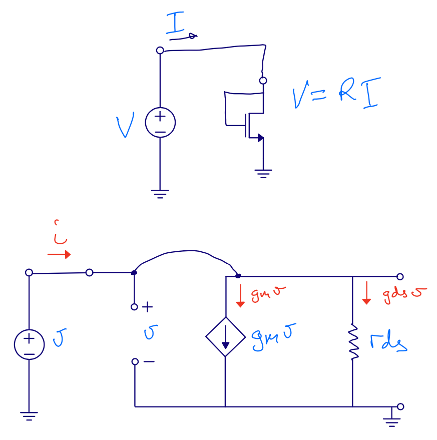


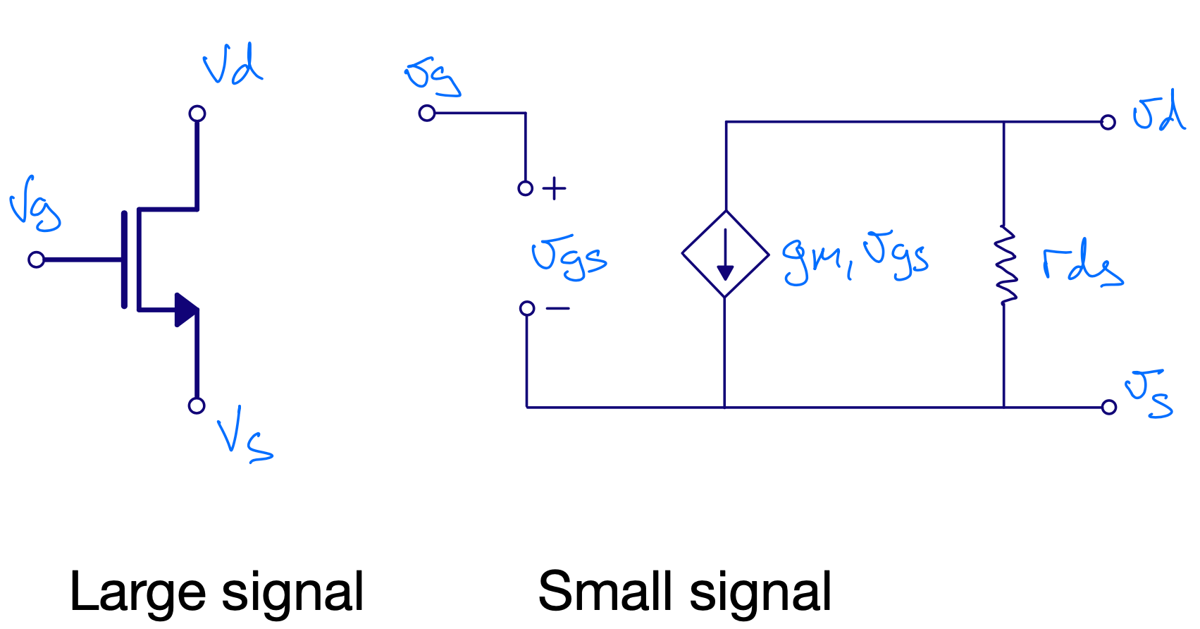
M1 is diode connected (VG = VD)
$$ r_{ds} = \frac{1}{g_{ds}} $$
$$ r_{in} = \frac{v}{i} $$
i = gmv + gdsv
$$ r_{in} = \frac{1}{gm + gds} \approx \frac{1}{gm} $$

| ## Current mirror rout |
| Output voltage does not affect vgs |
| rout = rds |
 |
What is the operating region of M3 and M4?
What is the operating region of M1 and M2?


vgs1 = 0
vgs2 = − vs
i = gds1vs ⇒ vs = irds1
$$r_{out} = \frac{v}{i}$$
$$i = -g_{m2} v_{s} + \frac{v - v_s}{r_{ds2}}$$

$$i = -g_{m2} v_{s} + \frac{v - v_s}{r_{ds2}}$$ insert vs = irds1
$$i = -i g_{m2} r_{ds1} + \frac{v - i r_{ds1}}{r_{ds2}}$$
irds2 + igm2rds1rds2 + irds1 = v
$$ r_{ds2} + g_{m2}r_{ds1}r_{ds2} + r_{ds1} = \frac{v}{i} $$
$$ r_{out} = r_{ds2} \left[1 + r_{ds1} \left( \frac{1}{r_{ds2}} + g_{m2}\right )\right] $$
rout = rds2[1+rds1(gm2+gds2)]

rout = rds2[1+rds1(gm2+gds1)]
Same equation as source degeneration, but M2 is in saturation
rds2(saturation) > rds2(linear)
rout = rds4[1+rds2(gm4+gds2)]
“High speed, high gain OTA in a digital 90nm CMOS technology” Berntsen, Wulff, Ytterdal
| ## Source follower |
| Input resistance ≈ ∞ |
| Gain $$ A = \frac{v_o}{v_i}$$? |
| Output resistance rout? |
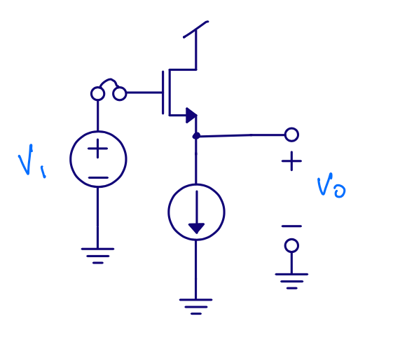 |


io = vo(gds+gs) − gmvi + vogm
io = 0
gmvi = vo(gm+gs+gds)
$$ A = \frac{v_o}{v_i} = \frac{g_m}{g_m + g_{ds} + g_s} $$

io = vo(gds+gs) − gmvi + vogm
vi = 0
io = vo(gds+gs+gm)
$$ r_{out} = \frac{v_o}{i_o} = \frac{1}{g_m + g_{ds} + g_{s}} $$
$$ r_{out} \approx \frac{1}{g_m}$$

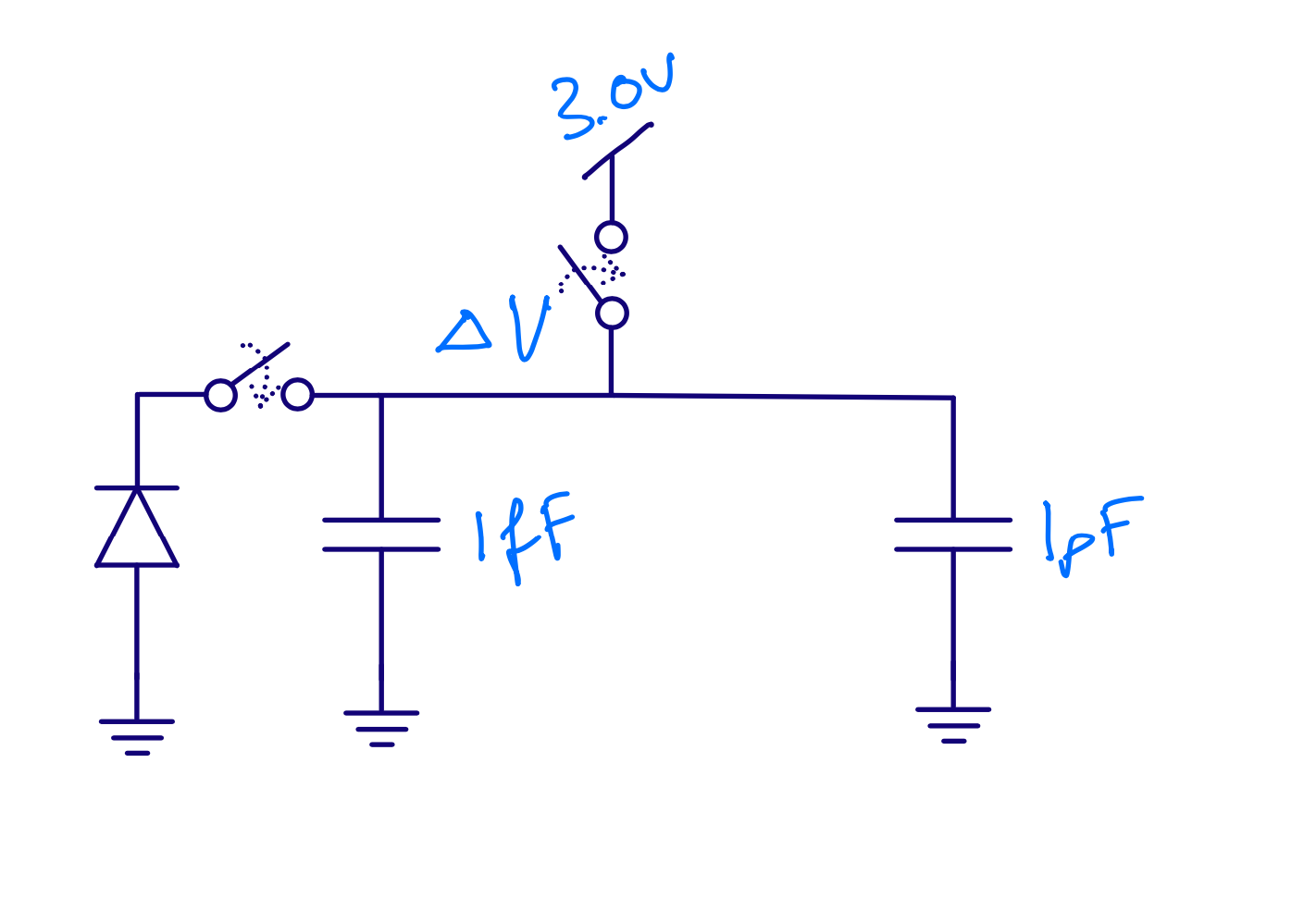
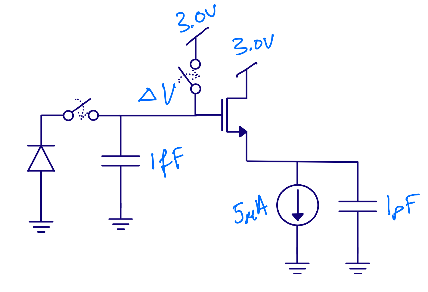
Assume 100 electrons
ΔV = Q/C = − 1.6 × 10−19 × 100/(1×10−15) = − 16 mV

ΔV = Q/C = − 1.6 × 10−19 × 100/(1×10−12) = − 16 uV

Input resistance ?
Gain ?
Output resistance ?
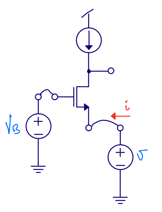


i = gmv + gdsv
$$ r_{in} = \frac{1}{g_m + g_{ds}} \approx \frac{1}{g_m}$$
However, we’ve ignored load resistance.
$$ r_{in} \approx \frac{1}{g_m}\left(1 + \frac{R_L}{r_{ds}}\right) $$


rout = rds


$$ i_{o} = - g_m v_{i} + \frac{v_{o} - v_{i}}{r_{ds}} $$
io = 0
0 = − gmvirds + vo − vi
vi(1+gmrds) = vo
$$ \frac{v_o}{v_i} = 1 + g_m r_{ds} $$

We’ve ignored bulk effect (gs), source resistance (RS) and load resistance (RL)
$$ A = \frac{(g_{m} + g_s + g_{ds})(R_L||r_{ds})}{1 + R_S\left(\frac{g_m + g_s + g_{ds}}{1 + R_L/r_{ds}}\right)}$$
If RL > > rds, RS = 0 and gs = 0
$$ A = \frac{(g_{m} + g_{ds})r_{ds}}{1} = 1+ g_m r_{ds} $$

Input resistance rin ≈ ∞
Output resistance rout = rds, it’s same circuit as the output of a current mirror
Gain ?
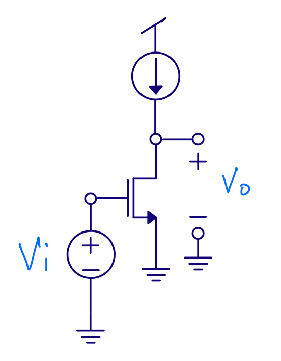


| ## Common source - Gain |
| $$ i_{o} = g_m v_i + \frac{v_o}{r_{ds}} $$ |
| io = 0 |
| $$ -g_m v_i = \frac{v_o}{r_{ds}} $$ |
| $$ \frac{v_o}{v_i} = - g_m r_{ds}$$ |
 |

| ## Differential pair |
| Input resistance rin ≈ ∞ |
| Gain A = gmrds |
| Output resistance rout = rds |
| Best analyzed with T model of transistor (see CJM page 31) |
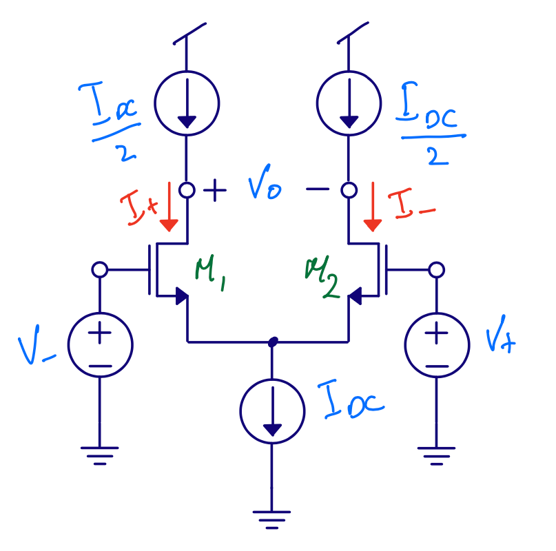 |

Can choose between
vo = gmrdsvi
and
vo = − gmrdsvi
by flipping input (or output) connections
