Table of contents
- The noise floor
- Three things that come in pieces
- Statistics
- Average Power
- Noise Spectrum
- Probability Distribution
- PSD of a white noise source
- Summing noise sources
- Signal to Noise Ratios
- Noise figure and Friis formula
- Spectral Density
- Where white noise comes from
- Where flicker noise comes from
- One trap
- What one trap looks like
- Which transistor in GR06?
- Many traps
- Summary
- Would you like to know more?
This chapter was written by Carsten Wulff and Claude, Anthropic’s AI, in collaboration. The statistics are Carsten’s; the physics of where noise comes from, and the reading of the GR06 trap, were drafted by Claude from Carsten’s outline and reviewed and edited by him.
The first part treats noise as statistics: a mean, a variance, a spectral density, and how they add through a circuit. The second part asks where the numbers come from. Thermal and shot noise take a slide each. Flicker noise takes the rest: we follow it all the way down to the single trap - one broken bond in the oxide that grabs an electron from the channel, holds it for a while, and lets it go. On a small transistor you can watch it happen, and on a chip from this course we do. Add up enough traps and you get the flicker noise of every MOSFET you will ever design with.
Every step of that story is quantum mechanics: Schrödinger gives the trap its wave function and the channel electron its tail into the oxide, and Pauli decides how traps fill. We will not solve anything hard. We will follow the chain, and put a number on each link.
The noise floor
Noise is a phenomenon that occurs in all electronic circuits. It places a lower limit on the smallest signal we can use. Many now have super audio compact disc (SACD)1 players with 24bit converters, 24 bits is around $2^{24} = 16.78$ Million different levels. If 5V is the maximum voltage, the minimum would have to be $\frac{5V}{2^{24}} \approx 298nV$. That level is roughly equivalent to the noise in a 50 Ohm resistor with a bandwidth of 96kHz. There exists an equation that relates number of bits to signal to noise ratio 2, the equation specifies that $SNR = 6.02*Bits + 1.76 = 146.24dB$. Back in 2005 the best digital to analog converter (DAC) that Analog Devices (a very big semiconductor company) had was a DAC with 120dB SNR, that equals around $Bits = (120-1.76)/6.02 = 19.64$. In other words, the last four bits of your SACD player is probably noise!
Three things that come in pieces
Classical physics has no noise floor. A classical charge fluid could be as smooth as you like. Real noise exists because three things come in pieces, and each piece gives one kind of transistor noise.
| What is discrete | Noise it gives |
|---|---|
| Charge, $q$ | Shot noise, $2qI$ |
| Energy per mode, $hf$ | Thermal noise, $4kTR$ |
| Localized states, traps | Telegraph noise, then $1/f$ |
The first part of this chapter is the statistics we need to describe any of them. Then we go looking for where they come from.
Statistics
The mean of a signal x(t) is defined as
\(\overline{x(t)} = \lim_{T\to\infty} \frac{1}{T}\int^{+T/2}_{-T/2}{ x(t) dt} \tag{1}\) The mean square of x(t) defined as
\(\overline{x^2(t)} =\lim_{T\to\infty} \frac{1}{T}\int^{+T/2}_{-T/2}{ x^2(t) dt} \tag{2}\) The variance of x(t) defined as
\(\sigma^2 = \overline{x^2(t)} - \overline{x(t)}^2 \tag{3}\) For a signal with a mean of zero the variance is equal to the mean square. The auto-correlation of x(t) is defined as
\[\begin{aligned} R_x(\tau ) &= \overline{x(t)x(t + \tau)} \\ &= \: \lim_{T\to\infty} \frac{1}{T}\int^{+T/2}_{-T/2}{ x(t)x(t+\tau) dt} \end{aligned}\]Average Power
Average power is defined for a continuous system by (4), and for discrete samples by (5).
$P_{av}$ usually has the unit $A^2$ or $V^2$, so we have to multiply/divide by the impedance to get the power in Watts. To get Volts and Amperes we use the root-mean-square (RMS) value which is defined as $\sqrt{P_{av}}$.
\[P_{av} = \lim_{T\to\infty} \frac{1}{T} \int^{+T/2}_{-T/2} x^2(t) dt \tag{4}\] \[P_{av} = \frac{1}{N}\sum_{i=0}^N x^2(i) \tag{5}\]If x(t) has a mean of zero then, according to (3), $P_{av}$ is equal to the variance of x(t).
Many different notations are used to denote average power and RMS value of voltage or current, some of them are listed in the two tables below. Notation can be a confusing thing, it changes from book to book and makes expressions look different.
It is important to realize that it does not matter how you write average power and RMS value. If you want you can invent your own notation for average power and RMS value. However, if you are presenting your calculations to other people it is convenient if they understand what you have written. In the remainder of this chapter we will use $\overline{e_n^2}$ for average power when we talk about voltage noise source and $\overline{i_n^2}$ for average power when we talk about current noise source. The n subscript is used to identify different sources and can be whatever.
| Voltage | Current |
|---|---|
| $V_{rms}^2$ | $I_{rms}^2$ |
| $\overline{V_n^2}$ | $\overline{I_n^2}$ |
| $\overline{v_n^2}$ | $\overline{i_n^2}$ |
| Voltage | Current |
|---|---|
| $V_{rms}$ | $I_{rms}$ |
| $\sqrt{\overline{V_n^2}}$ | $\sqrt{\overline{I_n^2}}$ |
| $\sqrt{\overline{v_n^2}}$ | $\sqrt{\overline{i_n^2}}$ |
Noise Spectrum
With random noise it is useful to relate the average power to frequency. We call this Power Spectral Density (PSD). A PSD plots how much power a signal carries at each frequency. In literature $S_x(f)$ is often used to denote the PSD. In the same way that we use $V^2$ as unit of average power, the unit of the PSD is $\frac{V^2}{Hz}$ for voltage and $\frac{A^2}{Hz}$ current. The root spectral density is defined as $\sqrt{S_x(f)}$ and has unit $\frac{V}{\sqrt{Hz}}$ for voltage and $\frac{A}{\sqrt{Hz}}$ for current.
The power spectral density is defined as two times the Fourier transform of the auto-correlation function 3
\(S_x(f) = 2\int_{-\infty}^{\infty}{R_x(\tau)e^{-j2\pi f \tau}d\tau} \tag{6}\) This can also be written as
\[\begin{aligned} S_x(f) &= 2\left[\int_{-\infty}^{\infty}{R_x(\tau)\cos(\omega \tau)d\tau} - \int_{-\infty}^{\infty}{R_x(\tau)j\sin(\omega \tau)d\tau}\right] \\ &= 2\left[\int_{-\infty}^{0}{R_x(\tau)\cos(\omega \tau)d\tau} +\int_{0}^{\infty}{R_x(\tau)\cos(\omega \tau)d\tau}\right] \\ &- 2j\left[\int_{-\infty}^{0}{R_x(\tau)\sin(\omega \tau)d\tau} + \int_{0}^{\infty}{R_x(\tau)\sin(\omega \tau)d\tau} \right] \\ &= 4\int_{0}^{\infty}{R_x(\tau)\cos(\omega \tau)d\tau} \\ &- 2j\left[- \int_{0}^{\infty}{R_x(\tau)\sin(\omega \tau)d\tau} + \int_{0}^{\infty}{R_x(\tau)\sin(\omega \tau)d\tau} \right] \\ &= 4\int_{0}^{\infty}{R_x(\tau)\cos(\omega \tau)d\tau} \end{aligned}\], since $e^{-j\omega \tau} = \cos(\omega \tau) - j \sin (\omega \tau)$, $R_x(\tau)$ and $\cos(\omega \tau)$ are symmetric around $\tau=0$ while $\sin(\omega \tau)$ is asymmetric around $\tau = 0$.
The inverse of power spectral density is defined as
\[R_x(\tau) = \frac{1}{2}\int_{-\infty}^{\infty}{S_x(f)e^{j 2 \pi f \tau} df} = \int_{0}^{\infty}{S_x(f) \cos(\omega \tau)df}\]If we set $\tau=0$ we get
\(\overline{x^2(t)} = \int_{0}^{\infty}{S_x(f)df} \tag{7}\) which means we can easily calculate the average power if we know the power spectral density. As we will see later it is common to express noise sources in PSD form.
Another very useful theorem when working with noise in the frequency domain is this
\(S_y(f) = S_x(f)\vert H(f)\vert ^2 \tag{8}\) , where $S_y(f)$ is the output power spectral density, $S_x(f)$ is the input power spectral density and $H(f)$ is the transfer function of a time-invariant linear system.
If we insert (8) into (7), with $S_x(f) = a:constant = D_v$ we get
\(\overline{x^2(t)} = \int{S_y(f)df} = D_v\int{\vert H(f)\vert ^2 df} = D_v f_x\) , where $f_x$ is what we call the noise bandwidth. For a single time constant RC network the noise bandwidth is equal to
\(f_x = \frac{\pi f_0}{2} = \frac{1}{4 R C}\) where $f_x$ is the noise bandwidth and $f_0$ is the 3dB frequency.
We haven’t told you this yet, but thermal noise is white and white means that the power spectral density is flat (constant over all frequencies). If $S_x(f)$ is our thermal noise source and $H(f)$ is a standard low pass filter, then (8) tells us that the output spectral density will be shaped by $H(f)$. At frequencies above the $f_x$ in $H(f)$ we expect the root power spectral density to fall by 20dB per decade.
Probability Distribution
Theorem 1 (Central limit theorem). The sum of $n$ independent random variables subjected to the same distribution will always approach a normal distribution curve as $n$ increases.
This is a neat theorem, it explains why many noise sources we encounter in the real world are Gaussian.4 Take thermal noise for example, it is generated by random motion of carriers in materials. If we look at a single electron moving through the material the probability distribution might not be Gaussian. But summing probability distribution of the random movements with a large number of electrons will give us a Gaussian distribution, thus thermal noise is Gaussian.
PSD of a white noise source
If we have a true random process with Gaussian distribution we know that the autocorrelation function only has a value for $\tau=0$. From the definition of auto-correlation we have that
\[\begin{aligned} R_x(\tau ) &={} \lim_{T\to\infty} \frac{1}{T}\int^{+T/2}_{-T/2}{ x(t)x(t - \tau) dt} \\ &={} \left[ \lim_{T\to\infty} \frac{1}{T}\int^{+T/2}_{-T/2}{ x^2(t) dt} \right] \delta(\tau) \\ &={}\: \overline{x^2(t)}\delta(\tau) \end{aligned}\]The reason being that in a true random process $x(t)$ is uncorrelated with $x(t + \tau )$ for any $\tau \neq 0$. If we use (6) we see that
\[\begin{aligned} S_x(f) &=\: 2\int_{-\infty}^{\infty}{\overline{x^2(t)}\delta(\tau)e^{-j 2 \pi f \tau} d\tau} \\ &=\:2\overline{x^2(t)} \int_{-\infty}^{\infty}{\delta(\tau)e^{-j 2 \pi f \tau} d\tau} \\ &= 2\overline{x^2(t)} \end{aligned}\], since
\(\int{\delta(\tau)e^{-j 2 \pi f \tau} d\tau} = e^0 = 1\) This means that the power spectral density of a white noise source is flat, or in other words, the same for all frequencies.
Summing noise sources
Summing noise sources is usually trivial, but we need to know why and when it is not. If we write the time dependant noise signals as
\(v_{tot}^2(t) = (v_1(t) + v_2(t))^2 = v_1^2(t) + 2v_1(t)v_2(t) + v_2^2(t)\) The average power is defined as
\[\begin{aligned} \overline{e_{tot}^2} &= \lim_{T\to\infty} \frac{1}{T}\int^{+T/2}_{-T/2}{ v_{tot}^2(t) dt} \\ &= \lim_{T\to\infty} \frac{1}{T}\int^{+T/2}_{-T/2}{ v_1^2(t) dt} \\ &+ \lim_{T\to\infty} \frac{1}{T}\int^{+T/2}_{-T/2}{ v_2^2(t) dt} \\ &+ \lim_{T\to\infty} \frac{1}{T}\int^{+T/2}_{-T/2}{ 2v_1(t)v_2(t) dt} \\ &= \overline{e_{1}^2} + \overline{e_{2}^2} + \lim_{T\to\infty} \frac{1}{T}\int^{+T/2}_{-T/2}{ 2v_1(t)v_2(t) dt} \end{aligned}\]If $\overline{e_{1}^2}$ and $\overline{e_{2}^2}$ are uncorrelated noise sources we can skip the last term in the sum above and just write
\(\overline{e_{tot}^2} = \overline{e_{1}^2} + \overline{e_{2}^2}\) Most natural noise sources are uncorrelated.
Signal to Noise Ratios
Signal to Noise Ratio (SNR) is a common method to specify the relation between signal power and noise power in linear systems. It is defined as
\[\begin{aligned} SNR &= 10 \log\left(\frac{Signal\:power}{Noise\:power}\right)\\ &= 10 \log\left(\frac{\overline{v_{sig}^2}}{\overline{e_{n}^2}}\right)\\ &= 20 \log\left(\frac{v_{rms}}{\sqrt{\overline{e_{n}^2}}}\right) \end{aligned}\]Another useful ratio is Signal to Noise and Distortion (SNDR), since most real systems exhibit non-linearities it is useful to include distortion in the ratio. One can calculate SNR and SNDR in many ways. If we don’t know the expression for $\overline{e_{n}^2}$ we can do a FFT of our output signal. From this FFT we sum spectral components except at the signal frequency to get noise and distortion. SNR is normally calculated as
\[SNR = 10 \log\left(\frac{Signal\:power}{Noise\:power\:-\:6 \:first\:harmonics}\right)\]And SNDR is calculated as
\[SNDR = 10\log\left(\frac{Signal\:power}{Noise\: power}\right)\]Noise figure and Friis formula
Noise factor is a measure on the noise performance of a system. It is defined as
\(F = \frac{\overline{v_o^2}}{source\:contribution\:to\:\overline{v_o^2}}\) where $\overline{v_o^2}$
is the total output noise. The noise figure is defined as (noise factor in dB)
\(NF = 10 \log(F)\) The noise factor can also be defined as
\[F = \frac{SNR_{input}}{SNR_{output}}\]This brings us right into what is known as Friis formula. The noise factor definition is only correct at room temperature, for more details, see 5. If we have a multistage system, for example several amplifiers in cascade, the total noise figure of the system is defined as
\[F = 1 + F_1 - 1 + \frac{F_2 -1}{G_{1}} + \frac{F_3-1}{G_{1}G_{2}} + ....\]Here $F_i$ is the noise figures of the individual stages and $G_i$ is the available gain of each stage. This can be rewritten as
\[F = F_1 + \sum_{i=1}^N{\frac{F_{i+1} - 1}{\prod_{k=1}^{i}{G_{k}}}}\]Friis’ formula tells us that it is the noise in the first stage that is the most important if $G_1$ is large. We could say that in a system it is important to amplify the noise as early as possible!
Spectral Density
Warning: This is not an introduction to spectral density. If the subject is completely unfamiliar I’d advise reading another source. For example chapter 4 in 2 or chapter 7 in 6.
Definition of Spectral Density
There are two different definitions of spectral density used in the literature. They differ by a factor of two. The one used in signal processing books, like 7, is
\(S_{x1}(f) = \int_{-\infty}^{\infty}{R_{x1}(\tau)e^{-j\omega\tau}d\tau}\) And the one often used in books about noise, like 3, is
\(S_{x2}(f) = 2\int_{-\infty}^{\infty}{R_{x2}(\tau)e^{-j\omega\tau}d\tau}\) In both cases $R_{xi}(\tau)$ is the auto-correlation function defined as
\(R_{xi}(\tau) = \overline{x_i(t)x_i(t+\tau)}\) As we can plainly see
\(S_{x1}(f) \neq S_{x2}(f)\) , there is no way these two can be made equal if
\(R_{x1}(\tau) = R_{x2}(\tau)\) This is ok, there is no problem having two different definitions for two different functions. In reality $S_{x1}(f)$ and $S_{x2}(f)$ are different functions of frequency, and we could say that
\(S_{x2}(f) = 2S_{x1}(f)\) if the two auto-correlation functions are equal.
Sources of Confusion
The problem with spectral density arises when reading literature from different communities, for example 7 and 3 where $S_x(f)$ is used for both $S_{x1}(f)$ and $S_{x2}(f)$. When I started investigating spectral densities this lead me to believe that different sources defined the same measure “spectral density” in two different ways. The more sources I investigated the more unsure I was about which of the two definitions that was correct. After months of searching (not actively, but sporadically) I eventually found the original source of the definition of spectral density 8. Having the original source helped, but I still don’t know when the original definition split into the $S_{x1}$ and $S_{x2}$ forms above. However, I’m pretty sure it’s just a matter of convenience. To see why the $S_{x2}$ form is the most common among sources concerning noise we look at the inverse Fourier Transform. By the way, if you had not noticed yet, both forms say that Spectral density is the Fourier Transform of the Auto-Correlation function. The inverse Fourier Transform of $S_{x1}$ is
\(R_{x1}(\tau) = \frac{1}{2\pi}\int_{-\infty}^{\infty}{S_{x1}(f)e^{j\omega\tau}dw} = \int_{-\infty}^{\infty}{S_{x1}(f)e^{j\omega\tau}df}\) ,since $dw = df dw/df = 2\pi df$. And for $S_{x2}$
\(R_{x2}(\tau) = \frac{1}{2}\int_{-\infty}^{\infty}{S_{x2}(f)e^{jw\tau}df}\) Before we proceed lets get rid of the $e$’s. We know that $e^{j\alpha} = \cos \alpha + j \sin \alpha$. So we could rewrite $S_{x1}$ as
\(S_{x1}(f) = \int_{-\infty}^{\infty}{R_{x1}(\tau)[\cos(\omega \tau) + j \sin( \omega \tau)]d\tau}\) and it turns out that since $R_{x1}(\tau)$ is an even function we can drop the $j\sin{\omega \tau}$ term. $S_{x1}(f)$ is also an even function since the Fourier Transform of an even function is even.
The definitions then become
\[\begin{aligned} S_{x1}(f) &= \int_{-\infty}^{\infty}{R_{x1}(\tau)\cos(\omega\tau)d\tau}\\ R_{x1}(\tau) &= \int_{-\infty}^{\infty}{S_{x1}(f)\cos(\omega\tau)df} \end{aligned}\]and
\[\begin{aligned} S_{x2}(f) &= 2\int_{-\infty}^{\infty}{R_{x2}(\tau)\cos(\omega\tau)d\tau}\\ R_{x2}(\tau) &= \frac{1}{2}\int_{-\infty}^{\infty}{S_{x2}(f)\cos(\omega\tau)df} \end{aligned}\]We can rewrite $R_{x2}(\tau)$ as
\(R_{x2}(\tau) = \overline{x_2(t)x_2(t + \tau)} = \int_0^{\infty}{S_{x2}(f)\cos(\omega\tau)df}\) and if $\tau = 0$
\(\overline{x_2^2(t)} = \int_0^{\infty}{S_{x2}(f)df}\) So using the $S_{x2}$ definition we see that average power (mean square value of $x_2(t)$) is equal to the integral from 0 to infinity of the spectral density. If we use $S_{x1}$ instead, average power would be
\(\overline{x_1^2(t)} = 2\int_0^{\infty}{S_{x1}(f)df}\) But if $R_{x1}(\tau) = R_{x2}(\tau)$ then
\(\overline{x_2^2(t)} = \overline{x_1^2(t)}\) even though $S_{x1}(f) \neq S_{x2}(f)$.
$S_{x1}$ is called the two-sided spectral density, and $S_{x2}$ the one-sided spectral density.
Example: Thermal Noise
The spectral density of thermal noise in electronic circuit should be known to anyone that has studied analog electronics. We normally define the voltage spectral density of thermal noise as
\(S_{th}(f) = 4kTR\) where k is Boltzmann’s constant, T the temperature in Kelvin and R the resistance. But that is the spectral density in the one-sided $S_{x2}$ definition. If we were to use the two-sided $S_{x1}$ definition, then the spectral density of thermal noise would be
\(S_{th}(f) = 2kTR\) Both these spectral densities would give the same average power value if we use the inverse Fourier Transform of the matching definition.9
Einstein: The source
In his 1914 paper 8 Albert Einstein described, supposedly for the first time, the auto-correlation function and what we have come to know as the spectral density. He defined the auto-correlation function as
\(\mathfrak{M} (\Delta) = \overline{F(t)F(t + \Delta)}\) and the intensity (spectral density) as
\(I(\theta) = \int_0^{T}{\mathfrak{M}(\Delta) \cos ( \pi \frac{\Delta}{\theta})d\Delta}\) ,where the period $\theta = T/n$ and $T$ is a very large value. The paper is very short, only 1 page, but it is worth reading. Note that the spectral density as the Fourier Transform of the auto-correlation function is often referred to as the Wiener-Khintchine theorem.
Where white noise comes from
Thermal noise is Planck
\[S_V(f) = 4R\frac{hf}{e^{hf/kT}-1} \approx 4kTR \quad \text{if } hf \ll kT\] \[\frac{kT}{h} = 6.25 \text{ THz at 300 K}\]Nyquist derived thermal noise in 1928 10, and he did not write $4kTR$. He wrote the Planck form above. A resistor in thermal equilibrium feeds energy into every electrical mode of the circuit around it, and each mode, being quantized in steps of $hf$, holds the Planck average energy. Below $kT/h$ every mode holds $kT$, and the density is flat.
At room temperature $kT/h$ is 6 THz. No circuit in this course gets near it, which is why we may forget Planck and write $4kTR$. A superconducting qubit at 10 mK has $kT/h$ = 200 MHz, and there the quantum correction is the whole design problem.
Shot noise is the electron charge
\[\overline{i_n^2} = 2qI\,\Delta f\]In weak inversion, with $\gamma = n/2$ and $g_m = I_D/nV_T$
\[4kT\gamma g_m = 4kT\frac{n}{2}\frac{I_D}{nV_T} = 2qI_D\]Current that crosses a barrier one electron at a time is a stream of independent arrivals, and the arrivals are random. That is shot noise.
In weak inversion the MOSFET is exactly that: electrons diffuse over the source barrier one at a time. Put the weak-inversion $\gamma$ and $g_m$ into the thermal noise formula and it becomes $2qI_D$. Thermal noise and shot noise in a subthreshold transistor are the same noise, described twice.
Where flicker noise comes from
Schrödinger
\[i\hbar\frac{\partial}{\partial t}\Psi(\vec{r},t) = \left[-\frac{\hbar^2}{2m}\nabla^2 + V(\vec{r})\right]\Psi(\vec{r},t)\]Stationary states, $\Psi = \psi(\vec{r})e^{-iEt/\hbar}$
\[-\frac{\hbar^2}{2m}\nabla^2\psi + V\psi = E\psi\]The wave function $\Psi$ is a probability amplitude: $\vert\Psi\vert^2$ is the probability of finding the electron at $\vec{r}$. The potential $V$ is everything the electron feels - the silicon nuclei, the other electrons, the gate field.
Three solutions of this equation carry the whole chapter. In a periodic crystal it gives energy bands, and near a band edge the electron moves as if free, with an effective mass. In the surface well of an inverted MOSFET it gives subbands, and the “2d sheet” of the MOSFET chapter. And at a broken bond it gives a bound state: a wave function localized to an atom or two, with an energy in the bandgap. That is a trap.
The equation has one more thing to say, and we need it. Where $E < V$ the solution does not stop. It decays as $e^{-\kappa x}$, with $\kappa = \sqrt{2m(V-E)}/\hbar$. The electron has a tail inside the barrier.
Fermi-Dirac
\[f(E) = \frac{1}{1 + e^{(E - E_F)/kT}}\] \[n = \int_{E_C}^{\infty} N(E) f(E)\, dE\]The probability that a state at energy $E$ holds an electron. Electrons have spin $\frac{1}{2}$, and Pauli allows at most one electron per quantum state, so they fill states by Fermi-Dirac and not by Boltzmann. The MOSFET chapter used it to count the electrons in the conduction band: the density of states $N(E)$, from Schrödinger, times the occupation $f(E)$. We will use it again in two places: to decide which traps can switch, and to find out where the $kT$ in flicker noise comes from.
One trap
What a trap is
- A broken bond at the Si/SiO2 interface, or a defect a few nm into the oxide
- A bound state: $\psi_T$ localized to an atom or two
- An energy $E_T$ inside the silicon bandgap
Silicon and its oxide do not fit perfectly. At the interface some silicon atoms are left with a bond that has no partner - a dangling bond - and the amorphous oxide has its own defects, oxygen vacancies and strained bonds, a few nanometres deep. Solve Schrödinger’s equation around one and you get a bound state: a wave function localized to an atom or two, at an energy inside the bandgap.
The channel electron has a tail
\[\psi_{ch}(x) \propto e^{-\kappa x} \text{ in the oxide}, \quad \kappa = \frac{\sqrt{2 m_{ox}(\Phi_B - E)}}{\hbar}\] \[\Phi_B = 3.1 \text{ eV}, \quad m_{ox} \approx 0.5 m_0 \Rightarrow \kappa \approx 6.4 \text{ nm}^{-1}\]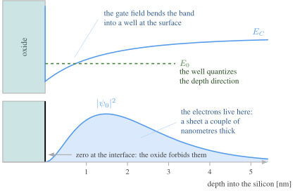
Figure 1: The inversion layer in depth, from the MOSFET chapter. The density is drawn as zero at the interface - the oxide forbids the electrons there - but forbids is too strong. A small tail leaks into the oxide
The MOSFET chapter drew the inversion electrons in the lowest subband of the surface well, with a density that goes to zero at the oxide. It is close to zero, not zero. The oxide is a barrier 3.1 eV high, and the Schrödinger equation inside a barrier gives an exponential.
Put the numbers in: with an effective mass in the oxide of half the free electron mass, $\kappa$ is 6.4 per nanometre. The probability density goes as $\vert\psi\vert^2 \propto e^{-2\kappa x}$, and falls a decade every 0.18 nm. Small, but a trap one nanometre into the oxide still overlaps the channel.
Tunnelling sets the time constant
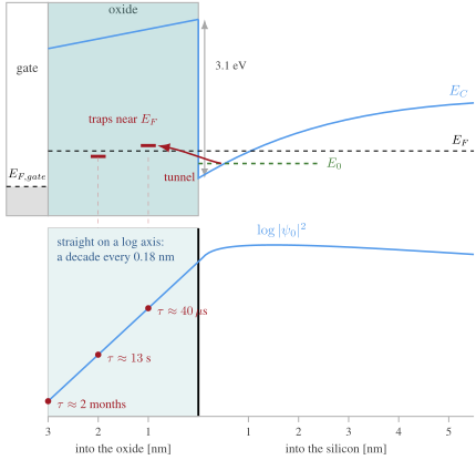
Figure 2: Above: a trap in the oxide with its level near the Fermi level can swap an electron with the channel. Below: the channel electron density on a log axis. In the oxide it is a straight line, a decade every 0.18 nm, and the time constant of a trap is set by where on that line it sits
An electron in the channel and an empty trap at depth $x_T$ are two states with almost the same energy, coupled through the overlap of their wave functions. The rate of hopping from one to the other is proportional to the channel density at the trap. Figure 2 shows the consequence: time constants that span microseconds to months, from traps a nanometre apart.
Dirac’s golden rule
\[\frac{1}{\tau} = \frac{2\pi}{\hbar}\left\vert\langle\psi_T\vert H'\vert\psi_{ch}\rangle\right\vert^2 \rho(E)\] \[\left\vert\langle\psi_T\vert H'\vert\psi_{ch}\rangle\right\vert^2 \propto e^{-2\kappa x_T}\] \[\tau = \tau_0 e^{x_T/\lambda}, \quad \lambda = \frac{1}{2\kappa} \approx 0.08 \text{ nm}\]| Trap depth | $\tau$ ($\tau_0$ = 0.1 ns) |
|---|---|
| 0 nm | 0.1 ns |
| 1 nm | 40 µs |
| 2 nm | 13 s |
| 3 nm | 2 months |
The rate of a transition is the squared matrix element between the two states times the density of final states. Dirac worked it out in 1927 11, in his own bra-ket notation; Fermi later called it a “golden rule”, and the name stuck to Fermi. The trap wave function is tiny, so the matrix element samples the channel wave function where the trap sits, and the squared matrix element inherits $e^{-2\kappa x_T}$.
The table is the punchline. Three nanometres of oxide hold sixteen decades of time constant. No other mechanism in a transistor produces a spread like that, and it is exactly what $1/f$ noise needs, as we will see. The prefactor $\tau_0$ is rough - textbooks quote 0.1 ns give or take a decade - but the slope is set by the barrier, and that is the part that matters. McWhorter used the same tunnelling picture in 1957 12, twenty years before anyone saw a single trap.
The lattice must move
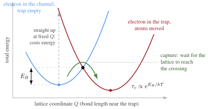
Figure 3: The configuration coordinate diagram. The trap is empty on the blue curve and full on the red one, and the atoms around a full trap sit somewhere else. The electron can only hop where the curves cross, so it waits for a thermal fluctuation of the lattice to get there
Tunnelling is not the whole story, and the measurements say so: trap time constants depend strongly on temperature, and tunnelling through an oxide barrier barely does.
The missing piece is the atoms. When a trap captures an electron its charge changes, and the bonds around it stretch or bend to suit. The total energy - electron plus lattice - is a parabola in the lattice coordinate, and there is one parabola for the empty trap and another for the full one, shifted sideways. The electron cannot drop straight from one to the other: at a fixed lattice position the full state costs more energy than the electron has, and the lattice cannot absorb the difference in one go. The hop happens where the two curves cross, and the lattice reaches the crossing only by a thermal fluctuation.
That wait is $e^{E_B/kT}$. In golden-rule language, the density of final states $\rho(E)$ now counts lattice vibrations - phonons - and the overlap of lattice states before and after is what makes the rate thermally activated. Henry and Lang worked out this multiphonon capture in 1977 13.
Capture and emission
\[\frac{1}{\tau_c} \propto e^{-x_T/\lambda}\, e^{-E_B/kT}\, n_s\] \[\frac{\tau_c}{\tau_e} = \frac{1}{g}e^{(E_T - E_F)/kT}, \quad g = 2\] \[\frac{\partial \ln(\tau_c/\tau_e)}{\partial V_{GS}} = -\frac{q}{kT}\frac{x_T}{t_{ox}}\]Capture needs an electron in the channel near the trap, so its rate grows with the inversion density $n_s$. Beyond that it is the product of the two factors we have: tunnel to depth $x_T$, and wait for the lattice.
Emission is the reverse trip, and the ratio of the two is fixed by thermal equilibrium: the trap must be occupied with the Fermi-Dirac probability. An empty trap can accept an electron of either spin, and a second electron costs extra Coulomb energy, so it belongs to a different level further up. “Full” is two quantum states and “empty” is one: that is the factor $g = 2$.
A trap only switches if $E_T$ is within a few $kT$ of $E_F$. Far below, it is always full; far above, always empty; either way it is silent.
The gate moves $E_F$ past $E_T$. In strong inversion the surface potential is pinned, so extra gate voltage drops across the oxide, and a trap a fraction $x_T/t_{ox}$ of the way to the gate sees that fraction of it. Measure $\tau_c/\tau_e$ against $V_{GS}$, and the slope tells you how deep the trap is. Kirton and Uren made a catalogue of traps this way 14.
What one trap looks like
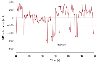
Figure 4: Sixty seconds of the GR06 temperature sensor from the measurement chapter, slow drift removed. The reading sits on one level, drops by about 0.6 K to another, stays a second or two, and returns
This is a chip from this course. The temperature sensor’s output is not a fuzzy band but two levels, which is what a single trap would do: empty, or full. The sensor turns currents and voltages into a temperature reading, so the step shows up in kelvin. Whether it really is a trap, and in which transistor, is a question we come back to once we know how big one trap’s step can be.
Ralls and colleagues first saw the same thing in the drain current of small MOSFETs in 1984 15. It goes by three names: random telegraph noise, popcorn noise, and burst noise.
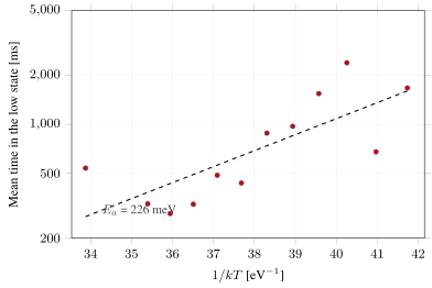
Figure 5: The GR06 trap’s mean time in the low state against inverse thermal energy. A straight line is an Arrhenius law, with an activation energy of 226 meV
And here is the lattice, measured. The time the trap stays in one state falls exponentially with temperature: a straight line against $1/kT$, slope 226 meV. Tunnelling alone would give a time constant almost independent of temperature. The 226 meV is the $E_B$ of Figure 3 plus the Fermi-Dirac shift of the previous slide - the lattice has to move before the electron can.
Not one Gaussian
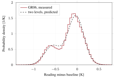
Figure 6: Two hours of the GR06 reading against its slow baseline. One trap gives two Gaussians, 534 mK apart, weighted 72 % and 28 % by the time spent in each state, each as wide as the 183 mK noise inside a state. The dashed line is that sum, not a fit
The central limit theorem of the first part says that many small independent sources add up to a Gaussian. One trap is not many sources. Its amplitude has two values, and the white noise of the sensor blurs each of them into a Gaussian of its own. A histogram is the quickest test there is for a telegraph signal hiding in a noisy reading.
Two states, one Lorentzian
\[R_x(\tau) = \Delta I^2 \frac{\tau_c\tau_e}{(\tau_c + \tau_e)^2} e^{-\vert\tau\vert/\tau_0}, \quad \frac{1}{\tau_0} = \frac{1}{\tau_c} + \frac{1}{\tau_e}\] \[S_x(f) = 4\int_0^\infty R_x(\tau)\cos(\omega\tau)d\tau = \frac{4\,\Delta I^2}{(\tau_c+\tau_e)\left[\left(\frac{1}{\tau_c}+\frac{1}{\tau_e}\right)^2 + (2\pi f)^2\right]}\]From here on the quantum mechanics is done, and we are back in the statistics of the first part. A trap has two states, and the time it spends in each is random, with means $\tau_c$ and $\tau_e$. Since the trap has no memory of how long it has waited, the autocorrelation decays exponentially. Fourier transform it with the one-sided definition from the first part and you get a Lorentzian: flat below the corner $f_0 = 1/(2\pi\tau_0)$, falling as $1/f^2$ above it. Machlup worked it out in 1954 16.
The factor $\tau_c\tau_e/(\tau_c+\tau_e)^2$ is the variance of a coin that lands full a fraction $f_T$ of the time, $f_T(1-f_T)$. It is largest when $E_T = E_F$ and the coin is fair.
The Lorentzian, measured
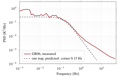
Figure 7: The spectrum of the same two hours, as measured. The dashed line is Machlup’s Lorentzian with the measured step and dwell times, not a fit: flat below 0.15 Hz, falling as $1/f^2$ above. The slow temperature drift rises below 30 mHz. Above 1 Hz the reading has more than one trap: short visits the detector misses, and the sensor’s own noise
Put the step, 534 mK, and the two mean dwell times, 3.7 s and 1.4 s, into the formula on the previous slide, and you have a prediction of the spectrum with nothing left to adjust. It lands on the measurement: the plateau, the corner and the $1/f^2$ slope. The dwell times come from counting edges in the time domain, the spectrum from a Fourier transform of the raw reading, and the Lorentzian ties the two together.
How big is one step?
\[\Delta V_T = \frac{q}{C_{ox}WL}\left(1 - \frac{x_T}{t_{ox}}\right), \quad \Delta I_D = g_m \Delta V_T\]| W x L | $\Delta V_T$ | $\Delta I_D/I_D$ at $g_m/I_D$ = 20 |
|---|---|---|
| 0.42 µm x 0.15 µm | 305 µV | 0.6 % |
| 1 µm x 1 µm | 19 µV | 0.04 % |
| 10 µm x 10 µm | 0.19 µV | 0.0004 % |
sky130 nfet_01v8: $t_{oxe}$ = 4.148 nm, $C_{ox}$ = 8.3 fF/µm²
One electron in the oxide images one electron’s worth of charge onto the gate and the channel. Seen from the gate it is a threshold shift $q/(C_{ox}WL)$, slightly less for a trap deep in the oxide, and the drain current moves by $g_m$ times that. The oxide thickness is in the model card: sky130’s 1.8 V nfet has an electrical oxide thickness $t_{oxe}$ of 4.148 nm, the pfet 4.23 nm, which with $\varepsilon_{ox} = 3.9\varepsilon_0$ is 8.3 and 8.2 fF/µm².
In a minimum-size sky130 transistor that is a third of a millivolt - more than half a percent of the current, from a single electron. Measured steps are often larger still, because the current does not flow evenly across the channel and a trap sitting on a busy path blocks more than its share. The charged trap also scatters the electrons that pass it, so mobility fluctuates along with the number of carriers. Hung’s unified model combines the two effects 17.
How many traps?
Per decade of time constant
\[N \approx N_t \cdot kT \cdot W L \cdot \lambda \ln 10\]$N_t = 4 \times 10^{17}$ cm$^{-3}$eV$^{-1}$ (sky130 nfet), $kT$ = 26 meV, $\lambda$ = 0.1 nm
| W x L | Active traps per decade |
|---|---|
| 0.42 µm x 0.15 µm | 0.15 |
| 1 µm x 1 µm | 2.4 |
| 10 µm x 10 µm | 240 |
A trap is only noisy if its level is near $E_F$ and its time constant is inside the band you care about. Weighted by how noisy each one is, the energy window is $kT$ wide (we will meet that integral again). A decade of time constant is $\lambda\ln 10$ of depth, about a quarter of a nanometre. So count the traps in a slab that thick and $kT$ wide.
The trap density is in the model card too, if you know where to look. Read through Hung’s model, the flicker noise parameter NOIA of sky130’s nfet is 2.5e42 J$^{-1}$m$^{-3}$, which is $4 \times 10^{17}$ cm$^{-3}$eV$^{-1}$; the pfet’s 1.5e42 is $2.4 \times 10^{17}$. The next part of the chapter shows why the noise parameter is a trap density.
The count is the point. A minimum-size transistor has, on average, about one active trap per seven decades of time constant. Most such devices are quiet, and the unlucky one has a large telegraph signal. Noise on small devices is not a number but a distribution, and it varies from device to device like mismatch does. Large devices have hundreds of traps per decade, and their steps blur into something smooth.
Which transistor in GR06?
How GR06 works
- A PTAT current, divided by 100 in two mirrors, charges a 53.8 fF MIM capacitor
- A comparator trips when the ramp reaches $V_{ref} = V_{DD}/3$, from three poly resistors
- Pulse width $t = C V_{ref}/I \approx$ 7.1 µs, so $I \approx$ 4.5 nA
- Every analog transistor is a 3.2/0.94 µm unit, deep in weak inversion; the reset switch is 1.92/0.22
Before blaming a transistor, write down what the pulse width depends on. A step of 0.53 K at 304 K is a fractional step of 1760 ppm in the pulse width. That is 1.06 mV at the comparator input, or 0.18 % of the charging current.
The reference is a resistive divider from the supply. Anything that steps the supply by 0.18 % - 3 mV - would look exactly like a trap. That is the first suspect to rule out.
Is it the supply?
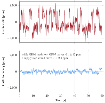
Figure 8: One minute of GR06 and GR07, recorded together on the same die, as fractional deviations on the same scale. While GR06 reads low, GR07 moves $-11 \pm 12$ ppm. A supply step would have moved it $-1763$ ppm
GR07, the other sensor on the die, compares against $V_{DD}/4$ from its own divider and reports a frequency instead of a width. A fractional supply step moves both by the same amount, with opposite signs. So record both at once, label each moment by GR06’s state, and ask how far GR07 moves between the two labels.
It moves $-11 \pm 12$ ppm. The error bar comes from the data: slide GR06’s labels 20 s to 400 s against GR07, where nothing real can line up, and the same calculation scatters by 12 ppm. A supply step would have given $-1763$ ppm. The supply is less than about 2 % of the step.
Memoryless
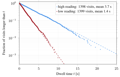
Figure 9: Two hours of GR06 at about 31 °C, cut into 2797 visits to the two levels. The fraction of visits that lasted longer than $t$ falls as a straight line on a log axis, over three decades - an exponential. The dashed lines are exponentials with the measured means, not fits
A trap has no memory: the chance it lets go in the next millisecond does not depend on how long it has held on. That makes the dwell times exponential, and a log survival plot turns an exponential into a straight line. Both levels give one, down to one visit in a thousand.
The two means put the Lorentzian corner at 0.15 Hz, the corner of Figure 7.
The suspects
| Device | W/L [µm] | $\Delta V_T$, one electron | $\Delta t/t$ |
|---|---|---|---|
| Comparator input pair | 4 x 3.2/0.94 | 1.6 µV | 3 ppm |
| Comparator load | 3.2/0.94 | 6.4 µV | 11 ppm |
| Reset switch, off leakage | 1.92/0.22 | 46 µV | < 1 ppm |
| PTAT core | 3.2/0.94 | 6.4 µV | 30 to 90 ppm |
| Ramp current mirror unit | 3.2/0.94 | 6.4 µV | 190 ppm |
| Measured | 1760 ppm |
$C_{ox}$ = 8.2 fF/µm² (pfet), 8.3 fF/µm² (nfet), from $t_{oxe}$ in the sky130 model cards; $nV_T$ = 34 mV
Every number in the last column is one electron’s $\Delta V_T = q/(C_{ox}WL)$, carried through to the pulse width.
The comparator is the least likely culprit. Its input pair is the largest device in the sensor, so one electron shifts its offset by 1.6 µV, and the step needs 1.06 mV. Its load refers to the input at about the same weight as the pair, because both run at the same current in weak inversion.
The reset switch is small, but it is off during the ramp. It leaks about 2 pA against 4.5 nA, and one electron changes that leakage by a tenth of a percent.
The current path is the best candidate. Each of the three single units that carry the ramp current - the PTAT output and the two hundredfold-division mirrors - converts a threshold step straight into current, $\Delta I/I = \Delta V_T/nV_T$, because in weak inversion $g_m/I_D = 1/nV_T$. That is 190 ppm, nine times short of the measurement.
Nine times is not a contradiction. The $\Delta V_T$ formula assumes the charge is spread evenly over the gate. In weak inversion it is not: the random dopants leave a lumpy barrier, the current crowds into the low spots, and a trap above one of them removes more than its share. The trapped charge also scatters the electrons that pass it 17. Both push the step up, and in weak inversion they can push it up a lot. A 3 µm² pfet has about four active traps per decade of time constant, so one near a second is no surprise.
How to tell
| Source | Step $\Delta t/t$ vs $T$ | Step $\Delta t/t$ vs $V_{DD}$ |
|---|---|---|
| Comparator offset | constant | $\propto 1/V_{DD}$ |
| Supply | ruled out | ruled out |
| Weak inversion current | $\propto 1/T$ or faster | constant |
| Measured | falls, 2500 to 1750 ppm from 5 °C to 45 °C | not measured |
A threshold step is a fixed voltage. At the comparator it is compared with $V_{ref}$, so its fractional effect does not depend on temperature and scales as $1/V_{DD}$. In a weak-inversion mirror it is compared with $nkT/q$, so its fractional effect falls with temperature and does not care about the supply.
The chamber sweep of the measurement chapter has the temperature column. The fractional step falls from about 2500 ppm at 5 °C to 1750 ppm at 45 °C - faster than $1/T$, and the points scatter, but it falls. That points at the current path. Above 50 °C the two levels merge into the noise and the step estimate is biased low, so those points are left out.
The supply column would settle it. Run the board’s core supply at a few voltages around 1.8 V: a step that stays at 1760 ppm is in the current path, a step that scales as $1/V_{DD}$ is at the comparator.
Many traps
McWhorter: uniform in depth is $1/f$
\[\tau = \tau_0 e^{x/\lambda} \Rightarrow dx = \lambda\frac{d\tau}{\tau}\] \[S(f) \propto \int_{\tau_1}^{\tau_2} \frac{\tau}{1 + \omega^2\tau^2}\frac{d\tau}{\tau} = \frac{1}{\omega}\left[\arctan(\omega\tau)\right]_{\tau_1}^{\tau_2} \approx \frac{\pi}{2\omega}\]for $1/\tau_2 \ll \omega \ll 1/\tau_1$
Spread the traps evenly in depth. Each one contributes a Lorentzian, $\tau/(1+\omega^2\tau^2)$. Since $\tau$ is exponential in depth, an even spread in depth is an even spread in $\ln\tau$: as many traps per decade of time constant at a microsecond as at a second. Add up the Lorentzians, and the sum is exactly $1/f$ between the slowest and the fastest trap.
This is McWhorter’s model 12. It needs nothing exotic - just traps scattered through the oxide, and the exponential that Schrödinger put in the tail of the channel electron.
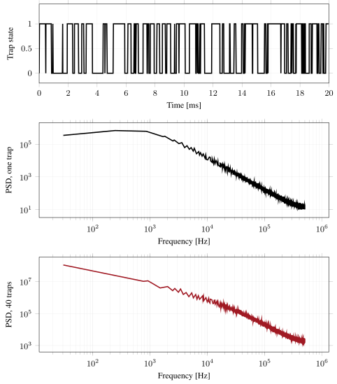
Figure 10: A single trap gives a two-level random telegraph signal (top) whose spectrum is a Lorentzian, flat then falling as $1/f^2$ (middle). Forty traps with time constants spread over three decades sum to a straight $1/f$, measured slope $-1.02$ between 100 Hz and 10 kHz (bottom)
The same argument, done numerically. Nothing was fitted: forty Lorentzians spread evenly in $\log\tau$, added. Above the corner of the fastest trap the slope steepens back towards $1/f^2$, because there are no faster traps left. A real flicker noise spectrum ends the same way, for the same reason.
Back to the design equation
\[S_{V_G}(f) = \frac{q^2\, kT\, \lambda\, N_t}{W L\, C_{ox}^2\, f}\]- $\lambda$: Schrödinger, the tunnelling length
- $kT$: Fermi-Dirac, $\int f(1-f)\,dE = kT$
- $N_t$: the process, how broken the oxide is
- $1/WL$: more traps, each smaller - $WL \times (1/WL)^2$
Do the McWhorter integral with every factor kept and you get the number-fluctuation model of flicker noise. It is the $K_f/(WLC_{ox}f)$ of the MOSFET chapter’s noise equations, with $K_f$ opened up.
Every factor is a piece of this chapter. The $\lambda$ is the 0.08 nm tunnelling length. The $kT$ is not thermal noise sneaking in: it is the width of the energy window where traps switch, since only traps near $E_F$ are noisy and the variance of each, $f_T(1-f_T)$, integrates over energy to exactly $kT$. The $N_t$ is the process. And the $1/WL$ is the competition between more traps and smaller steps: a bigger device has more traps, proportional to $WL$, but each step in $V_T$ shrinks as $1/WL$, and power goes as the step squared.
That is why flicker noise falls with gate area and nothing else in the hand formula, and why a PMOS, with its holes a little further from the interface, is often quieter.
The model card knows
BSIM4, flicker noise model 1, as used by ngspice:
\[S_{I_D} \propto \frac{q^2\, kT\, \mu\, I_D}{10^{10}\, f^{EF} A_{bulk} C_{oxe} L^2} \left[\text{NOIA} \ln(\ldots) + \ldots\right]\]| sky130 01v8 | $t_{oxe}$ | NOIA [J$^{-1}$m$^{-3}$] | $N_t$ [cm$^{-3}$eV$^{-1}$] | EF |
|---|---|---|---|---|
| nfet | 4.148 nm | 2.5e42 | $4.0 \times 10^{17}$ | 0.84 |
| pfet | 4.23 nm | 1.5e42 | $2.4 \times 10^{17}$ | 1.0 |
The simulator’s flicker noise model is this chapter, compiled. BSIM4’s unified model is Hung’s 17, and Hung’s is McWhorter’s number fluctuation plus the mobility fluctuation of a charged trap. The constant $10^{10}$ in the denominator is not a fudge: it is the tunnelling attenuation coefficient, $1/\lambda$ in metres, so the simulator assumes $\lambda$ = 0.1 nm, close to our 0.08 nm. The $kT$ is the Fermi-Dirac window. And NOIA, the parameter the foundry fits to measured noise, is the trap density $N_t$ in J$^{-1}$m$^{-3}$ - divide by the electron charge to get eV.
EF is the exponent of $f$. The pfet’s is 1, McWhorter’s ideal. The nfet’s is 0.84: its spectrum falls slower than $1/f$, so it has more fast traps than an even spread would give. In the tunnelling picture the traps are not uniform in depth - they crowd towards the interface, where the time constants are short.
So the next time a simulation hands you a flicker noise corner, you know what it is made of: a trap density, a tunnelling length, a Fermi window and an area.
Summary
The one-page version of this chapter:
- Noise is random: describe the amplitude by its distribution (usually Gaussian) and the power by its spectral density
- Integrate the density over the band you keep to get the power the signal must beat; uncorrelated sources add in power
- Friis: with gain up front, only the first stage’s noise matters - spend your current there
- Thermal noise is Planck, $4kTR$ below 6 THz; in weak inversion it is shot noise, $2qI$
- Flicker noise comes from traps: a bound state in the oxide, reached by tunnelling, a decade of time constant per 0.18 nm of depth
- Capture also moves the lattice, which makes it Arrhenius - 226 meV on GR06
- One trap is a telegraph signal: two Gaussians, exponential dwell times, a Lorentzian - all three measured on GR06
- Many traps, even in depth, are $1/f$; small transistors have few, so their noise varies from device to device
- The simulator’s flicker model is the same physics: sky130’s NOIA is a trap density, 4e17 per cm³ per eV
Would you like to know more?
The classic on noise in solid state devices, still the reference 3
Friis’ original, short and still the clearest statement of why the first stage decides the noise figure 5
Chapter-length treatments of circuit noise, either of which will do 6 2
The random walk that thermal noise is made of, from the source 8, and thermal noise from Planck, in the original 10
The review of individual traps in MOSFETs, and the place to start 14
The first clear observation of single traps in silicon inversion layers 15
The tunnelling model of $1/f$ noise 12, and the spectrum of a two-state signal 16
Multiphonon capture, the reason traps are thermally activated 13
Number and mobility fluctuation combined into one flicker noise model 17
Dirac’s golden rule 11. The equation all of this physics comes from is the QED Lagrangian in the refresher chapter
A curiosity: the trapped electron has a spin, and with microwaves at its resonance it can be read out through the drain current of one transistor 18
-
This paragraph is from the mid-2000s, when music came on discs. The compact disc (CD), launched by Philips and Sony in 1982, stores two channels of 16-bit samples at 44.1 kHz, read from a spinning disc by a laser. The super audio CD (SACD), from the same two companies in 1999, stores the music as a 1-bit sigma-delta stream at 2.8224 MHz, 64 times the CD rate - the oversampled, noise-shaped signal of the chapter on sigma-delta ADCs. Both have since given way to streaming, but the argument stands: a 24-bit converter promises more than any circuit can deliver. ↩
-
David Johns and Ken Martin, Analog Integrated Circuit Design 1997 ; ↩ ↩2 ↩3
-
Aldert Van Der Ziel, Noise in Solid State Devices and Circuits 1986 ; ↩ ↩2 ↩3 ↩4
-
Gaussian distribution = normal distribution. Gaussian describes the amplitude distribution; white describes a flat spectral density. Thermal noise happens to be both. ↩
-
Friis, H.T., Noise Figures of Radio Receivers 1944 https://doi.org/10.1109/JRPROC.1944.232049 ↩ ↩2
-
Behzad Razavi, Design of Analog CMOS Integrated Circuits 2001 ↩ ↩2
-
Robert M. Gray and Lee D. Davisson, An Introduction to Statistical Signal Processing 2004 ↩ ↩2
-
Albert Einstein, Method for the Determinination of the Statistical Values of Observations Concerning Quantities Subject to Irregular Fluctuations 1987 ; ↩ ↩2 ↩3
-
Note that if you calculate the average power of $S_{th}(f)$ you’ll get infinity. You have to include the bandwidth of the circuit you are considering for average power to have a finite value. ↩
-
H. Nyquist, Thermal agitation of electric charge in conductors 1928 https://doi.org/10.1103/PhysRev.32.110 ↩ ↩2
-
P. A. M. Dirac, The quantum theory of the emission and absorption of radiation 1927 https://doi.org/10.1098/rspa.1927.0039 ↩ ↩2
-
A. L. McWhorter, 1/f noise and germanium surface properties 1957 ↩ ↩2 ↩3
-
C. H. Henry and D. V. Lang, Nonradiative capture and recombination by multiphonon emission in GaAs and GaP 1977 https://doi.org/10.1103/PhysRevB.15.989 ↩ ↩2
-
M. J. Kirton and M. J. Uren, Noise in solid-state microstructures: A new perspective on individual defects, interface states and low-frequency (1/f) noise 1989 https://doi.org/10.1080/00018738900101122 ↩ ↩2
-
K. S. Ralls and W. J. Skocpol and L. D. Jackel and R. E. Howard and L. A. Fetter and R. W. Epworth and D. M. Tennant, Discrete resistance switching in submicrometer silicon inversion layers: individual interface traps and low-frequency (1/f?) noise 1984 https://doi.org/10.1103/PhysRevLett.52.228 ↩ ↩2
-
S. Machlup, Noise in semiconductors: spectrum of a two-parameter random signal 1954 https://doi.org/10.1063/1.1721637 ↩ ↩2
-
K. K. Hung and P. K. Ko and C. Hu and Y. C. Cheng, A unified model for the flicker noise in metal-oxide-semiconductor field-effect transistors 1990 https://doi.org/10.1109/16.47770 ↩ ↩2 ↩3 ↩4
-
M. Xiao and I. Martin and E. Yablonovitch and H. W. Jiang, Electrical detection of the spin resonance of a single electron in a silicon field-effect transistor 2004 https://doi.org/10.1038/nature02727 ↩