The Project
If you find an error in what I’ve made, then fork, fix lectures/l01_project.md, commit, push and create a pull request. That way, we use the global brain power most efficiently, and avoid multiple humans spending time on discovering the same error.
AIC is likely one of the most rewarding courses I’ve attended at NTNU. It gave me a lot of valuable knowledge on different types of circuits, IC design workflows and open source EDA tools that I greatly appreciate. It is also one of the most challenging courses, due to the amount of effort and time I had to spend in order to figure things out. - Tord, AIC2025
A fantastic project/course that just might turn your world upside down, push you to re-evaluate your life choices, and stare briefly into the existential void… all while being deeply enjoyable and engaging! - Domen, AIC2025
The goal of the project is for you to experience a full mixed signal integrated circuit design, with the option of tapeout!
In 2025, two groups reached a tapeout of their design http://analogicus.com/jnw-tt-2025/ on the https://tinytapeout.com/chips/ttsky25a/ Tiny Tapeout shuttle.
Below is the layout of group 6 https://analogicus.github.io/jnw_gr06_sky130a/ and group 7 https://analogicus.github.io/jnw_gr07_sky130a/

Figure 1: Layout of group 6 and group 7 temperature sensors from AIC2025
The project will walk you through the full analog/digital design process. From specification all the way to a finished layout, and a potential tapeout.
The project is not easy, it’s rather hard. You’ll experience frustration, desperation, epic wins, epic losses, stress, collaboration, and you will figure out whether you love analog design, or digital design or neither.
I promise that the design project closely matches how we would develop a circuit in industry.
I ask a lot of you on the project, as such, it accounts for 45 % of the grade, and is maybe the thing that you’ll learn the most from.
In this document I’ll go through the problem (what we’re trying to solve), and the milestones that we’ll use along the way.
The problem
The assignment is
Design an oscillator that has a frequency that varies with temperature
But why? I’ll try to explain.
System-on-chip have complex regulator systems
See the example in Figure 2 from Nordic Semiconductor’s nRF54L15 product specification.
VDD is the supply from the battery (1.7 V - 3.6 V). While the DECD, DECA and DECRF are the low voltage supplies for the digital, analog and radio.
The VREGMAIN has both a DC/DC, and a LDO. We’ll learn about those in the course. For now it’s sufficient to know that the DC/DC converts power drawn on the low supply (DECA, DECD, DECRF) to power drawn from the high supply (VDD), while the LDO has the samme current on low supply as the high supply, but the voltage is different.
You will learn in the course that the typical systems inside VREGMAIN are complicated, and sometimes complex, analog circuits.
From the datasheet you’ll see that the lowest power state is about 700 nA, while the highest power state is about 10 mA. The high power state is 14 thousand times higher than the low power state!

Figure 2: Power system of nRF54L15
Those numbers are the total current consumption. That includes switching currents from digital, analog bias currents, and leakage currents. In modern technologies, because of the low threshold voltage, the leakage currents can be a large part of the total current budget.
Leakage current varies orders of magnitude over temperature
The sub-threshold leakage current in a MOSFET is
The change in leakage as a function of temperature is rather complicated. The $V_T = \frac{k T}{q}$ factor is easy, but both $I_0$ and $V_{th}$ have a complicated relation to temperature.
In Figure 3 you can see the leakage simulation (from http://analogicus.com/lelo_aic_sky130a/)

Figure 3: Leakage simulation
Based on the previous curves we could run a thought experiment.
-
Assume 1 pA at 25 C, and 1 nA at 125 C, per logic cell
-
Assume 100 million logic cells
-
Leakage at 25 C => 100 uA
-
Leakage at 125 C => 100 mA !!!
We would like to know the temperature on die
Expanding on the thought experiment.
-
Assume we use 1 % of the load current for the regulator
-
At 25 C => 1 uA for LDO
-
At 125 C => 1 mA for LDO
It’s insanely difficult to design a regulator that is efficient across the full range of leakage currents at any temperature.
It would be good if we could know temperature.
How to measure temperature?
There are a multitude of ways to make a temperature sensor. In [@tang20] they used a leakage based digital ring oscillator, in [@jeong2014] they used a two-transistor MOSFET sensing element, in [@pertijs2005] they had a more complicated sigma-delta ADC sensing bipolar transistors.
The design of a temperature sensor is signficiantly more difficult than you think. As such, I would suggest that you don’t go too crazy in your choice of sensor. So far, none has gotten close to the finish line with a sigma-delta ADC based sensor.
In the previous years of Advanced Integrated Circuits most groups have chosen an architecture similar to [@park2022] Fig. 2. I would recommend you do the same, and that’s what I’ll target in the milestones.
The principle of the temperature sensor is: 1) Create a current that is proportional to temperature (Lecture 3), 2) Convert current to frequency with a relaxation oscillator (Lecture 9). 3) Check the frequency to read the temperature.
The Project: Design a temperature sensor
| Parameter | Value | Unit | Description |
|---|---|---|---|
| Area | < 10 | km^2 | |
| Conversion time | < 30 | us | Analog should only be active for one 32768 Hz period |
| Sample rate | 100 | ms | |
| Leakage current | < 1 | nA | |
| Active current | < 100 | uA | |
| Average current | < 50 | nA | Active current x conversion time/sample rate + leakage current |
| Accuracy 0 - 70C | +-10 | C | One temperature (25C) calibration |
| Accuracy 0 - 70C | +-5 | C | Two temperature (25C, 85C) calibration |
Grade
Milestones are important, and Milestone 0 - 5 will count towards your final grade!
That means, you have to start working right away.
The points have been designed such that it’s impossible to get an A without getting some points on the layout
| Milestone | What does it mean | Condition for more than 0 points | Possible Points |
|---|---|---|---|
| M0 | You have completed the tutorial | Link on blackboard | 5 |
| M1 I=f(T) | Circuit that can convert a temperature into a current | Description of the sub circuit on github docs | 5 |
| M2 T=f(I) | Circuit that can convert a current into a frequency | Description of the sub circuit on github docs. Demonstrate that it works | 10 |
| M3 D=f(T) | A verilog testbench that can convert your frequency into a digital value | Description of the TB in README.md | 10 |
| M4 Layout | Layout of your circuit | DRC/LVS/GDS passing on github | 20 |
| M5 Report | Individual report | Uploaded to blackboard | 48 |
| Coolness | Extra points that I may choose to award | 10 | |
| Total | 108 |
Milestone 0: The tutorial
The goal of milestone 0 is to force you to install the tools, and get you started.
Follow: Sky130nm Tutorial
Submit link to your github repository on blackboard
For example, my repository: LELO_EX_SKY130A
The exercise will teach you the skills you need to do the project
Milestone 1:
The goal of the first milestone is to create a circuit that can transform a temperature on the IC to a current proportional to temperature (PTAT), and a voltage complementary to temperature (CTAT).
\[I = f(T)\]For this purpose it’s common to use “Bandgap” circuits. We’ll learn about them in the course, but if you don’t want to wait then you should read https://analogicus.com/aic2026/2026/01/09/Lecture-3-References-and-bias.html and ask me questions in reference and bias lecture.
In the git repository for your group you’ll create schematics for the bandgap circuits, and you’ll make testbenches to check that the bandgap circuit works.
If you don’t know what you should simulate, it’s good to have a chat to chat. See https://chatgpt.com/share/69481b11-8830-8007-9986-c9e41d735cfc.
Or check my testbenches at https://github.com/wulffern/lelo_temp_sky130a/tree/main/sim/LELOTEMP_BIAS_IBP
Delivery On blackboard link to your github repository with a description of how the bandgap works.
Milestone 2:
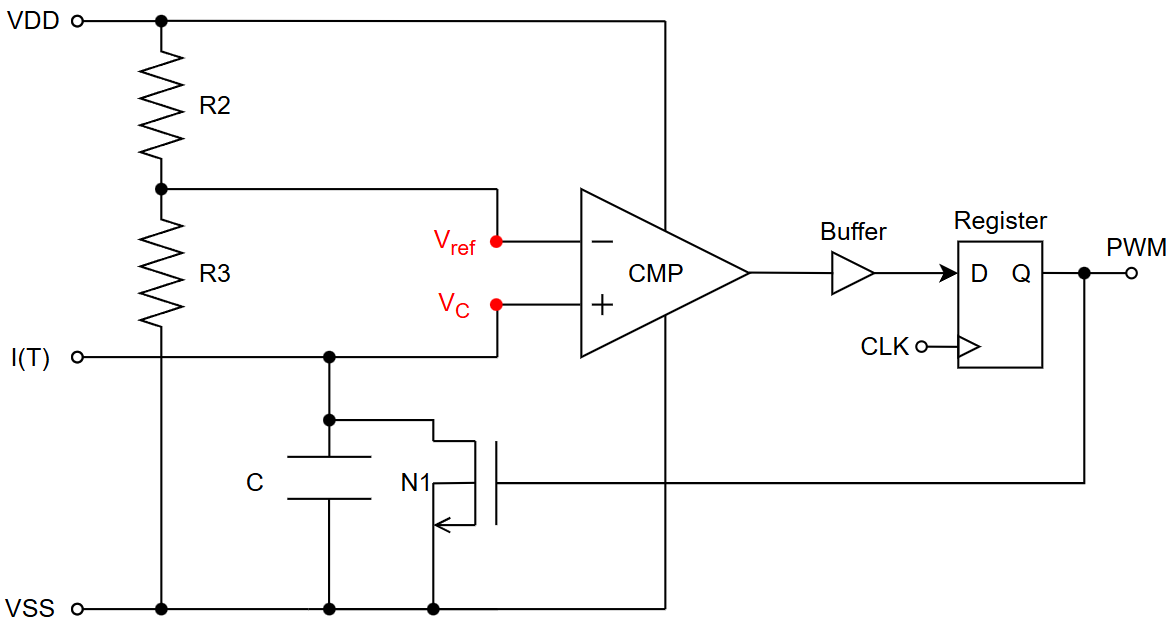
The goal of milestone 2 is to use the PTAT current, and the CTAT voltage an create a oscillator.
\[t = f(I)\]One way is to charge a capacitor with the current, and have a comparator trigger when the voltage on the capacitor reaches a voltage (CTAT voltage for example).
When the comparator triggers, then we can reset the capacitor. This is similar to what group 7 did last year (one of the groups got all the way to tapeout).
One difference, though, is that group 7 used VDD/2 as the reference. I would recommend you use the CTAT voltage from the bandgap instead. That way, the oscillation frequency is independent (to first order) from the VDD.
 Delivery On blackboard, link to your github repository with description on
how your oscillator works.
Delivery On blackboard, link to your github repository with description on
how your oscillator works.
Milestone 3:
The goal of milestone 3 is to figure out how to measure the frequency of the oscillator.
In the system we can assume we have an accurate 32768 Hz clock source. One way to find the frequency is to run the oscillator for a fixed number of clock cycles on the 32768 Hz clock, and have a counter that can count the output pulses.
Assume we counted 128 clock cycles over 2 clock periods of the 32768 Hz clock. That would mean the frequency of the oscillator was approximately 2.09 MHz. Once we have the frequency we can calculate the temperature.
I would recommend that you write in verilog the system to start the oscillator, count for a number of 32768 Hz clock cycles, and transform the frequency into a temeprature.
Delivery On blackboard, link to your github repository where you describe how you measure the frequency of the oscillator.
Milestone 4 (Optional):
The last design milestone is to do the physical layout of your oscillator, and prove that it still works with the layout parasitics.
Those students that follow the course at NTNU will be able to tapeout if the design is complete. I’ve gotten Nordic Semiconductor to sponsor the tapeout for 2026.
If you do the layout, then your design must fit within a digital 1x1 tinytapeout block. I’ve made a template at https://github.com/wulffern/lelo_temp_sky130a/blob/main/design/LELO_TEMP_SKY130A/tt_block_1x1_pg.mag that you can use. If the design does not fit within that space, then you won’t be able to tapeout.
When your design is complete, then the DRC, LVS, GDS actions should be passing on github.
Delivery On blackboard, link to your github repository with passing GDS, DRC, LVS actions.
Milestone 5:
The last milestone is the report. You shall deliver a PDF of the report in Inspera. You’ll all write an individual report. The report shall be in the IEEE template.
See further details in https://analogicus.com/aic2026/2023/10/26/How-to-write-a-project-report.html