Analog Design Fundamentals
If you find an error in what I’ve made, then fork, fix lectures/l01_ad.md, commit, push and create a pull request. That way, we use the global brain power most efficiently, and avoid multiple humans spending time on discovering the same error.
- Analog Design Process
- Flavors
- Picking transistor size
- State-of-the-art
- How to make state-of-the-art designs
- My only published state-of-the-art design
- Trigger
- Problem
- Architecture
- Question
- Plan
- How to make multiple SAR ADCs with limited time?
- Result
- SUN_SAR9B_GF130N
- Recommendations
- https://github.com/wulffern/aicex
- What \(gm/I_d\) would you pick?
Analog Design Process
- Define the problem, what are you trying to solve?
- Find a circuit that can solve the problem (papers, books)
- Find right transistor sizes. What transistors should be weak inversion, strong inversion, or don’t care?
- Check operating region of transistors (.op)
-
Check key parameters (.dc, .ac, .tran)
- Check function. Exercise all inputs. Check all control signals
- Check key parameters in all corners. Check mismatch (Monte-Carlo simulation)
- Do layout, and check it’s error free. Run design rule checks (DRC). Check layout versus schematic (LVS)
- Extract parasitics from layout. Resistance, capacitance, and inductance if necessary.
- On extracted parasitic netlist, check key parameters in all corners and mismatch (if possible).
- If everything works, then your done.
On failure, go back as far as necessary
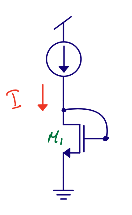
Assume active (\(V_{ds} > V_{eff}\) in strong inversion, or \(V_{ds} > 3 V_T\) in weak inversion) For diode connected transistors, this is always true
Weak inversion
\(I_{D} = I_{D0} \frac{W}{L} e^{V_eff / n V_T}\), \(V_{eff} \propto \ln{I_D}\)
Strong inversion
\(I_{D} = \frac{1}{2} \mu_n C_{ox} \frac{W}{L} V_{eff}^2\), \(V_{eff} \propto \sqrt{I_D}\)
Operating region for a diode connected transistor only depends on the current

Flavors
Mosfets come in flavors, we can separate into PMOS and NMOS.
Random 130 nm MOS technology
| Parameter | Min | Max | Unit |
|---|---|---|---|
| L | 0.13 | 100 | um |
| W | 0.15 | 50 | um |
Assume 5n quantization. Permutations per transistor (P) \(P = 2 \times 19974 \times 9970 = 398 \text{ M}\)
Typical ADC ~ 20 k transistors \(P_{ADC} = 20 \text{ k} \times 2 \times 398 \text{ M} = 16 \text{ P}\)
Too large solution space for exhaustive search
Picking transistor size
Not possible with exhaustive search
Simplify as much as possible
Use brain

State-of-the-art
How to make state-of-the-art designs
Know what is known
Find a good problem to solve
Find an architecture that could work
Work through all important details
If publishing, have some luck
There is no magic in state-of-the-art designs
However, a fast brain might get there faster. A slow brain may never reach the end.
My only published state-of-the-art design

Trigger
Back in November 2009 I was listening to Lanny Lewyn talk about regular layout at NorChip in Trondheim and idea struck ‘I’m pretty sure I’m able to write a script to generate this layout’. In 2010 I started writing the script.
Problem
Although I knew what I wanted to do, generate layout, I needed a problem to solve. It was not enough for me to make something to generate layout. I wanted the generated layout, and the generated analog blocks, to be better than anything out there. It should be state of the art, even though it was generated, or compiled.
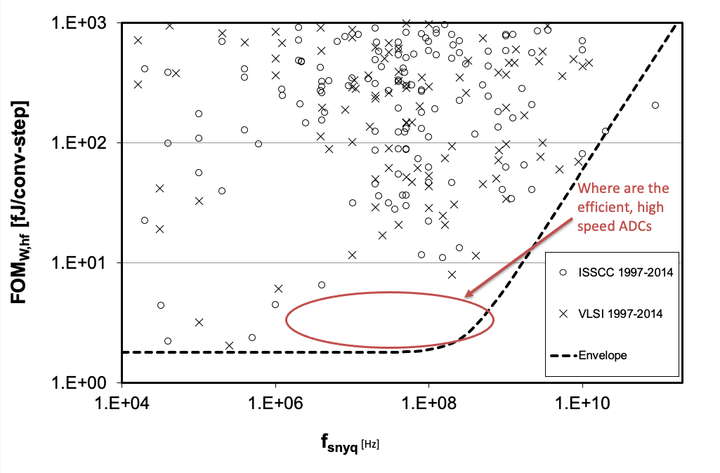
I don’t remember how I choose the problem, but I did see the overview of ADCs and noticed the lack of high efficiency, medium speed ADCs. I also knew from my PhD that Walden figure of merit favors low-resolution ADCs.
Architecture
In 2009 there was really only one type of ADC that made sense, the successive-approximation ADC. Using finger capacitors had become common, and it was demonstrated that it was OK to use really small capacitors, down to atto farads.
The thermal noise power of an ADC is in part determined by the capacitor size, given by
\[P_{noise} = \frac{k T}{C}\]Especially in nano-scale, and we were targeting 28 nm FDSOI, it was now possible to design both atto farad unit caps, and approach the thermal limit for 8-bit ADCs.
I was not sure whether it would be 8-bit, 9-bit or 10-bit that would be the most power optimum for 28 nm FDSOI, so I wanted to make multiple versions.
Question
Designing a SAR ADC from scratch takes times!
Could I design “once and for all” a process independent SAR architecture that is tolerant towards supply, temperature, process, mismatch and process technology?
Could I generate multiple versions, one 8-bit, 9-bit and 10-bit?
Plan
9-bit SAR ADC with 28 nm FDSOI transistors
9-bit SAR ADC with IO voltage (180 nm) FDSOI transistors

How to make multiple SAR ADCs with limited time?
Spend 50% of time for 6 months to develop a tool to make SAR ADCs
Spend 50% of time for 6 months to make the SAR ADCs
At the time, my language of choice was Perl, so the first version of the script was a 16 k line Perl program that I named cnano.
Cnano was started while I worked at Nordic, and I was able to bring the code with me to NTNU when I started my post doc.
In the end, cnano turned out out be slow, and the problem of variable type (numbers could be integer or float, but in a controlled manner) was becoming an issue.
As such, I started writing Custom IC Creator abbreviated cic (which actually meant Carstens IC creator ;-) ) in 2014. cic is written in C++, and was developed to replace cnano. After 2017, I stopped maintaining cnano.
Below is an exceprt of the cic code. You can download cic from https://github.com/wulffern/ciccreator
#include "core/layoutcell.h"

typedef QMap<QString,QList<cIcSpice::SubcktInstance*>>  SARgroup;

namespace cIcCells{

    class SAR : public cIcCore::LayoutCell
    {
        Q_OBJECT

    public:
        virtual void place();

        virtual void route();

        int getCellWidth(SARgroup groups,QString group);

        cIcCore::Instance* placeAlternateMirror(SARgroup groups,QString group,
            int i, int x ,int y, int xoffset);

        int addSarRouting(int y,int msw,int mw);

        static bool sortGraph(cIcCore::Graph* a, cIcCore:: Graph *b);

    private:
        Rect* sarn;
        Rect* sarp;
    };
}
I wanted the input data to cnano/cic to be human readable, easy to parse and independent of technology. I also wanted the input data to be independent of platform (linux,mac,windows) and CAD vendor (Cadence, Synopsys )

16 k Perl lines. Ported to C++ for speed \(\Rightarrow\) ciccreator
![]()


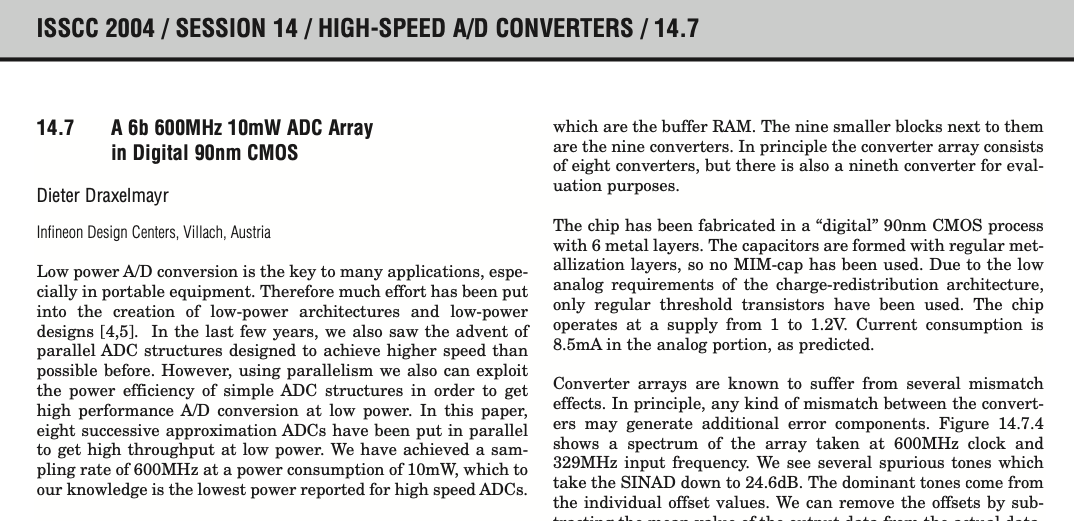
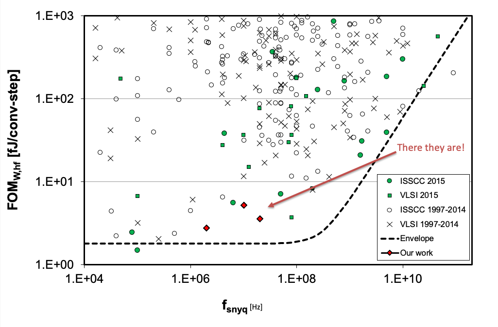
A Compiled 9-bit 20-MS/s 3.5-fJ/conv.step SAR ADC in 28-nm FDSOI for Bluetooth Low Energy Receivers


Result
SUN_SAR9B_GF130N
├── SAR9B_CV.json
├── SAR9B_CV.spi
├── capacitor.json
├── dmos_gf130nm_core.json
└── gf_130bcdlite.tech
9-bit is not the energy optimum for GF130N. The power consumption of the digital is too high. The energy optimum is more like 13-bit, however, the CDAC matching limits performance to about 10/11-bit
\[\log2[(W_{130n} L_{130n})/(W_{28n} L_{28n} )] = \log2[(0.95\times0.14)/(0.258 \times 0.03)]=4\text{-bit extra}\]
Recommendations
https://github.com/wulffern/aicex
Typical

Temperature

Process

Process and temperature

What \(gm/I_d\) would you pick?
Temperature and BINN 0 N1_0 i=i(VREF) tc1={0.3/100}

Process, Temperature and BINN 0 N1_0 i=i(VREF) tc1={0.3/100}

![]()