l3_pn
- TFE4152 - Lecture 3
- PN Junctions
- Goal for today
- Want to go deeper
- Computer models
- How do charge carriers in intrinsic silicon move?
- Drift and Diffusion
- n-type
- p-type
- Built in voltage
- Depletion widths
- Capacitance of forward bias
TFE4152 - Lecture 3
PN Junctions
Source
Goal for today
- Refresh what you should aready know about PN
- Carrier concentrations
- Built in voltage
- Reverse bias
- Forward bias
- Small signal models
Want to go deeper
\(q = 1.6 \times 10^{-19} [C]\) \(k = 1.38 \times 10^{-23} [J/K]\)
\[\mu_0 = \frac{2 \alpha}{q^2}\frac{h}{c} = 1.26 \times 10^{-6} [H/m]\] \[\epsilon_0 = \frac{1}{\mu_0 c^2} = 8.854 \times 10^{-12} [F/m]\]where q is unit charge, k is Boltzmann’s constant, h is Plancks constant, c is speed of light and alpha is the fine structure constant
from scipy import constants
import numpy as np
h = constants.physical_constants["Planck constant"][0]
k = constants.Boltzmann
q = constants.physical_constants["elementary charge"][0]
c = constants.c
alpha = constants.physical_constants["fine-structure constant"][0]

mu = 2* alpha*h/(c*np.power(q,2))
print("Permiability of free space = %g" % mu)

epsilon = 1/(mu* c**2)
print("Permitivity of free space = %g" % epsilon)
wulff@lectures$  python l3_constants.py
Permiability of free space = 1.25664e-06
Permitivity of free space = 8.85419e-12
Computer models
http://bsim.berkeley.edu/models/bsim4/
http://bsim.berkeley.edu/BSIM4/BSIM480.zip
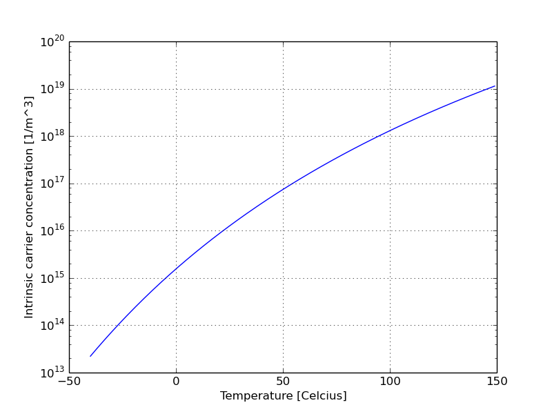
\(n_i \approx 1 \times 10^{16} [1/m^3] = 1 \times 10^{10} [1/cm^3]\) at 300 K
\[n_i^2 = n_0 p_0\] \[n_i = \sqrt{N_C N_V}e^{\frac{-E_g}{2kT}}\]\(N_C = 2\left(\frac{2 \pi m_{n}^* k T}{h^2}\right)^{3/2}\) \(N_V = 2\left(\frac{2 \pi m_{p}^* k T}{h^2}\right)^{3/2}\)
https://github.com/wulffern/dic2021/blob/main/2021-07-08_diodes/intrinsic.py
Solid state physics:
\[n_i = \sqrt{N_C N_V}e^{\frac{-E_g}{2kT}}\]BSIM 4.8, Intrinsic carrier concentration (page 122)
\[n_i = 1.45e10\frac{TNOM}{300.15}\sqrt{\frac{T}{300.15}}exp\left[21.5565981 - \frac{qE_g(TNOM)}{2 k_b T}\right]\]How do charge carriers in intrinsic silicon move?
Drift and Diffusion

n-type
\[n_n \approx N_D\] \[p_n = \frac{n_i^2}{N_D}\]p-type
\[p_p \approx N_A\] \[p_n = \frac{n_i^2}{N_A}\]PN junctions
Symbol
How carriers move
Carrier distribution
Depletion zone
Current characteristics
Avalanche
Built in voltage
\[\frac{n_n}{n_p} = e^{\frac{q \Phi_0}{kT}}\]where \(q \Phi_0\) is the energy required to climb the potential barrier, \(kT\) is the thermal energy, and \(n_n\) and \(n_p\) are the electron concentrations in the n-type and p-type.
\[\Phi_0 = V_T ln\left(\frac{N_A N_D}{n_i^2}\right)\] \[V_T = \frac{kT}{q}\]Depletion widths
\[x_n = \left(\frac{2 K_s \epsilon_0\Phi_0}{q} \left[1 + \frac{V_R}{\Phi_0}\right] \frac{N_A}{N_D ( N_A + N_D )}\right)^{l_1}\]where, \(K_s = 11.8\) is the relative perimittivity of silicon, and \(l_1 \approx 0.5\) to almost unity, depending on the doping profile
For \(x_p\) replace \(N_A = N_D, N_D = N_A\)
Junction capacitance of reversed bias junctions
CJM, single sided diode:
\[C_j = C_{j0} \left[ 1 + \frac{V_R}{\Phi_0}\right]^{-1/2}\]BSIM 4.8:
\[C_{jbs} = CJS(T)\left(1 - \frac{V_{BS}}{PBS(T)}\right)^{-MJS}\] \[CJS(T) = CJS(TNOM) + TCJ(T - TNOM)\] \[PBS(T) = PBS(TNOM) -TPB(T - TNOM)\]Small-Signal model under forward bias
Large signal current \(I_D = I_s (e^{V_D/V_T} -1)\)
Small signal conductance \(g_d = \frac{dI_D}{dV_D} = \frac{I_D}{V_T} = \frac{1}{r_d}\)
Capacitance of forward bias
\(C_j\) is similar (but not same) as reverse bias (page 106 in BSIM 4.8)
Additional term due to the increased minority carrier on the “other side”
\[C_d = \tau_T \frac{I_D}{V_T} = \frac{\tau_T}{r_d}\]\(C_T = C_j + C_d\) where \(\tau_T\) is the transit time of the diode