l2_manufacturing
- TFE4152 - Lecture 2
- Manufacture Integrated Circuits
- Goal for today
- Let’s make a battery charger
- How
- Printed Circuit Board (PCB)
- Package and Test
- Die
- Who makes dies?
- Wafer
- Quantum Bound States
- Photolithography
- EUV lithography
- Add stuff
- Remove stuff
- Diffusion
- How do we go from idea to GDSII?
- Want to learn more?
TFE4152 - Lecture 2
Manufacture Integrated Circuits
Source
- Learn to learn
- How did I choose analog
- Exam: December 10’th
Goal for today
- Why
- How
- What
Why
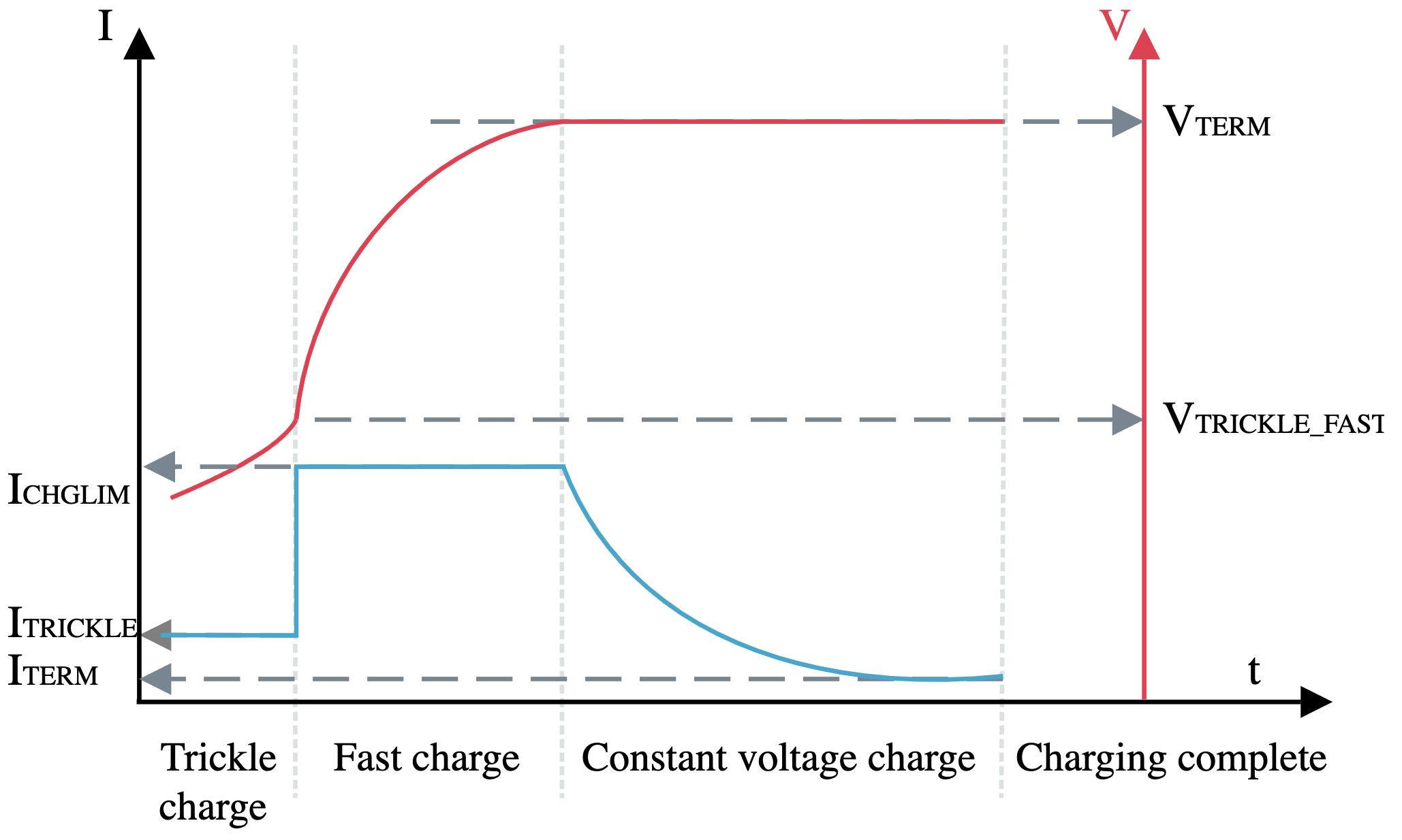
Let’s make a battery charger
How
- What does the use case require?
- What IC do we need?
- How is it connected to the real world?
- What pins do we need?
- What states are there?
How
Printed Circuit Board (PCB)
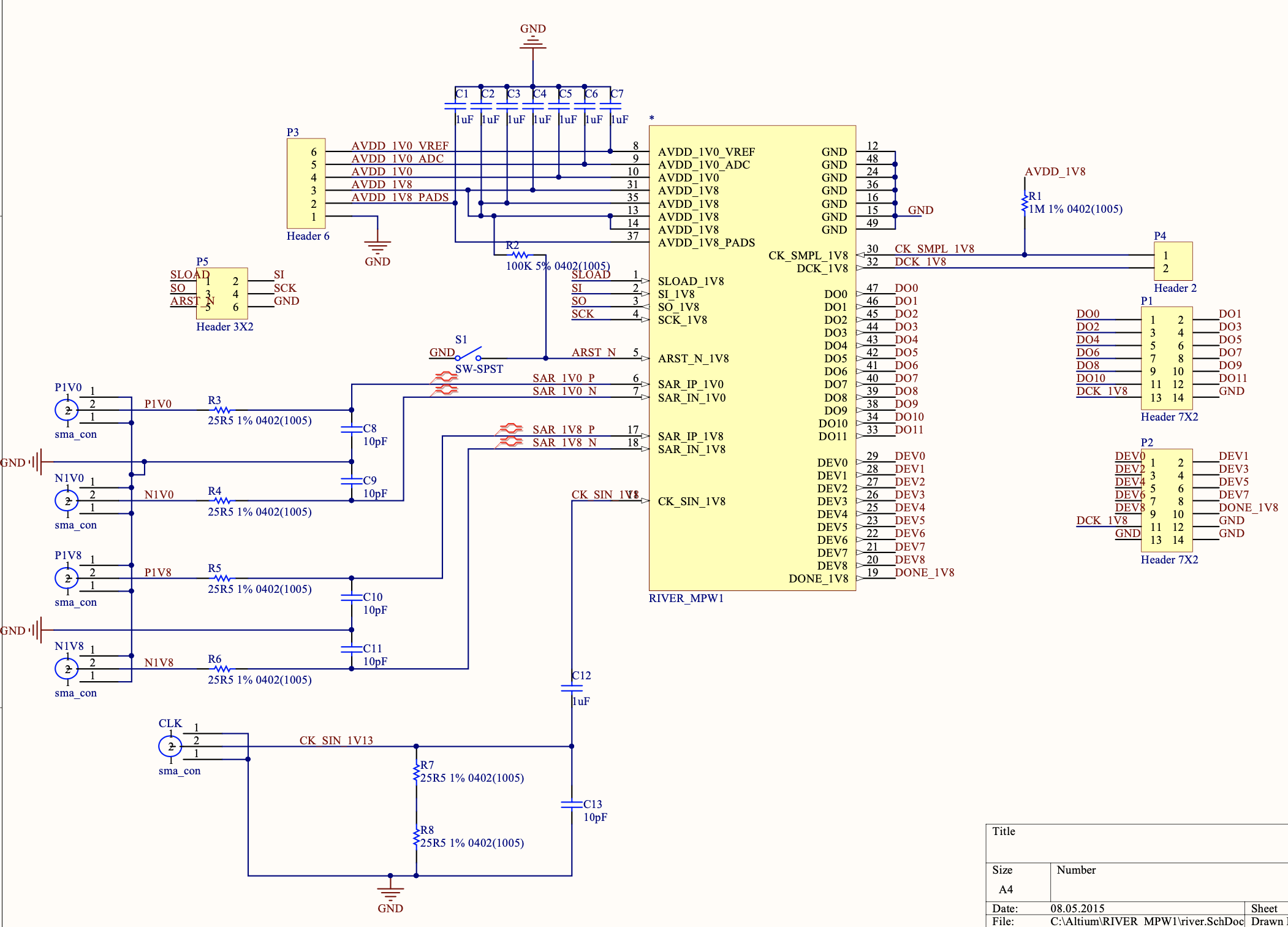
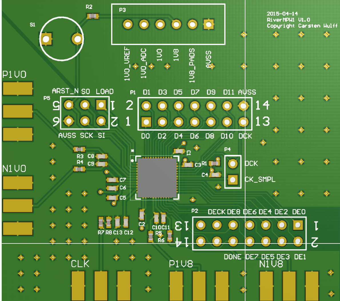
- Many, many vendors
- I know Ph.D that students have used PCBway
- Omega Verksted probably know best option
- Use Altium to design the PCB
Package and Test
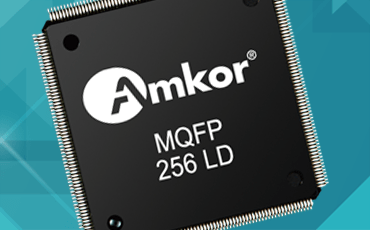
Many package options
Usually done by OSATS (Outsourced Semiconductor Assembly and Test)
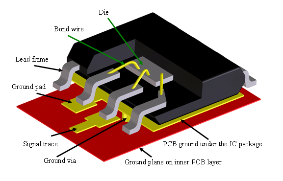 Online, https://www.iue.tuwien.ac.at/phd/poschalko/img410.png
Die
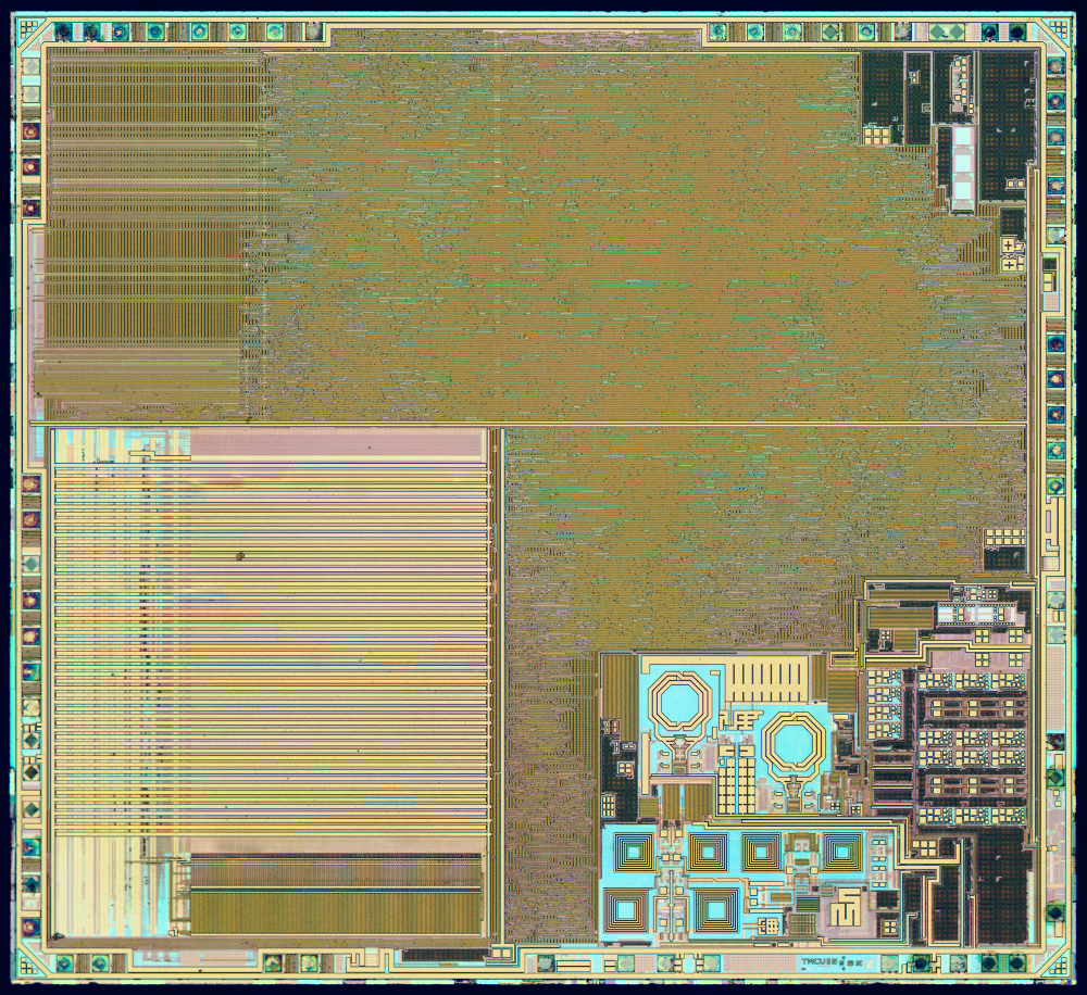 Picture: nRF51822 (https://s.zeptobars.com/nRF51822.jpg)
Who makes dies?
- TSMC, Globalfoundries, Samsung, UMC, SMIC …
- Extremely high initial cost (k$ to M$)
- Low production cost (« $ per mm2)
- Sam Zeloof, made one i his garage https://www.youtube.com/watch?v=IS5ycm7VfXg&t=3
Wafer
Ingot created with Czochralski Process

Quantum Bound States
Everything should be made as simple as possible, but no simpler. (A. Einstein)


Photolithography
ArFr light source: 193 nm
Resolution: < 38 nm
Wafers per hour: > 250
Overlay: < 2.0 nm
Price: Don’t know. Maybe 100 M$?
https://www.youtube.com/watch?v=ShYWUlJ2FZs

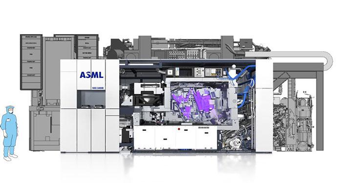
EUV lithography
Light source : 13.5 nm Resolution : ?? Wafers per hour : 100 ?? Price: ???
\(E = hf = hc/\lambda\), where \(h = 4.1e-15 eV/Hz\) and \(c = 3e8\)
| Wavelength [nm] | Energy [eV] |
|---|---|
| 1000 | 1.2 |
| 240 | 5.1 |
| 193 | 6.4 |
| 90 | 13.6 |
| 13.5 | 91.1 |
Seems like the highest known band gap is about 13.5 eV (Lithium Fluoride)
 Online, https://i1.wp.com/semiengineering.com/wp-content/uploads/2016/11/Screen-Shot-2016-11-15-at-4.04.00-PM.png?w=953&ssl=1

Add stuff
Remove stuff
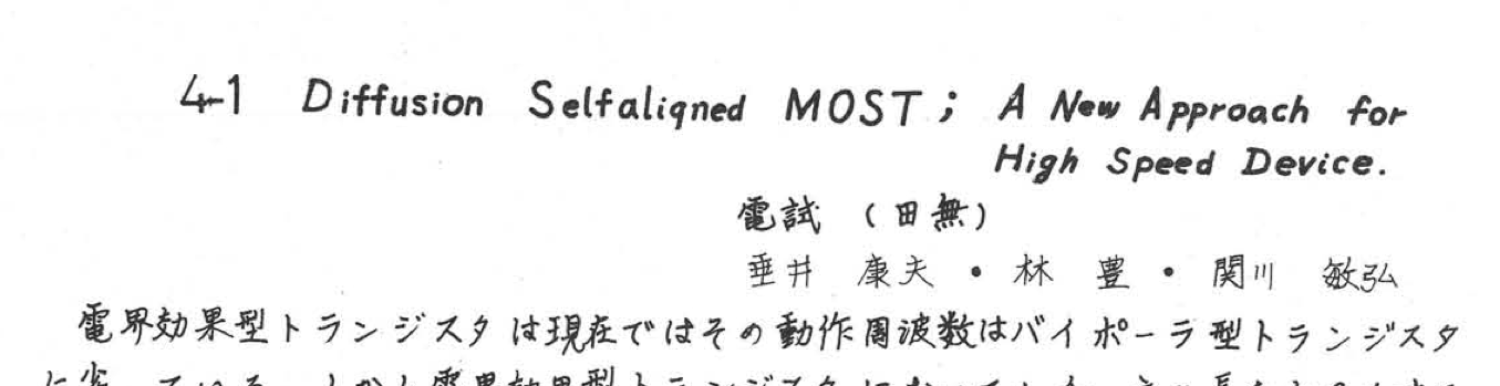
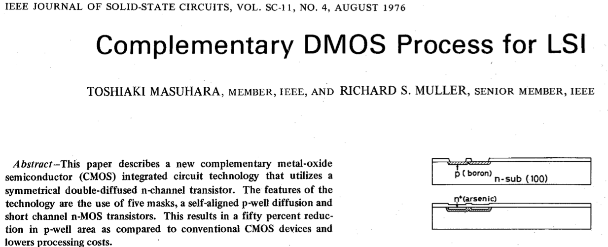
Diffusion
Diffusion Selfaligned MOST; A New Approach to High Speed Devices, 1969
Complementary DMOS Process for LSI
What

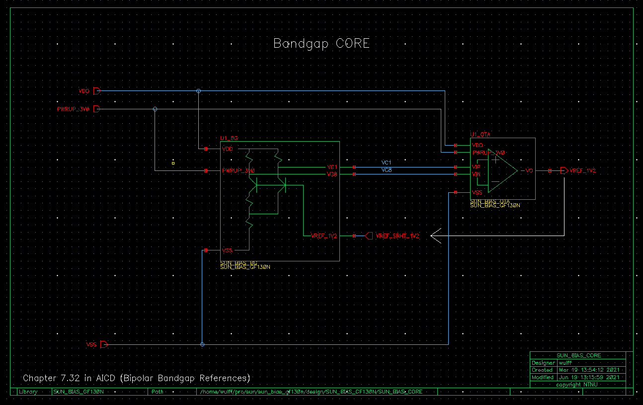
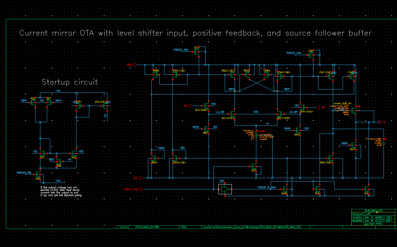
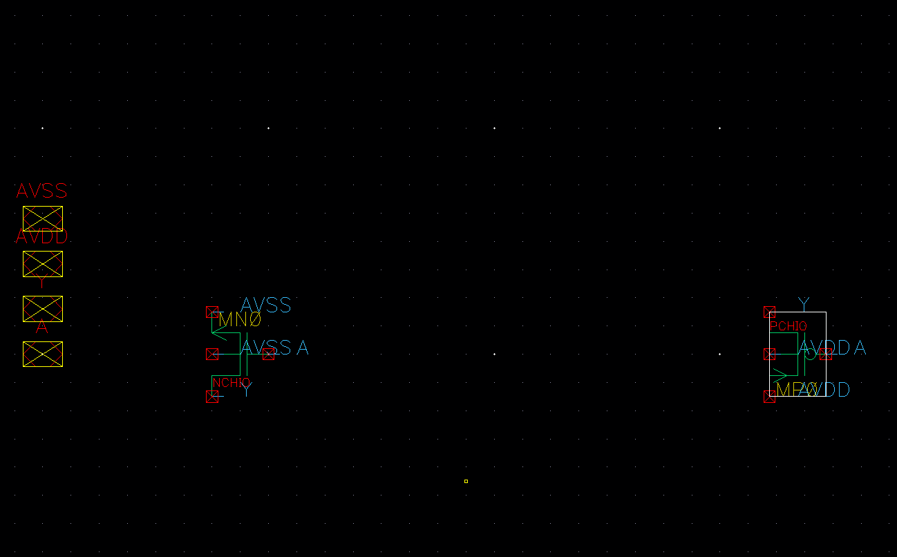
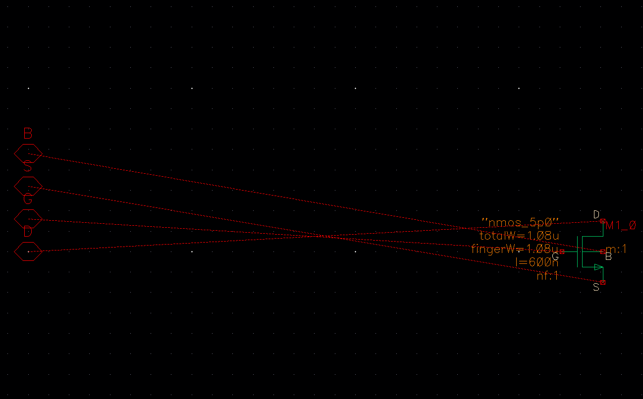
How do we go from idea to GDSII?
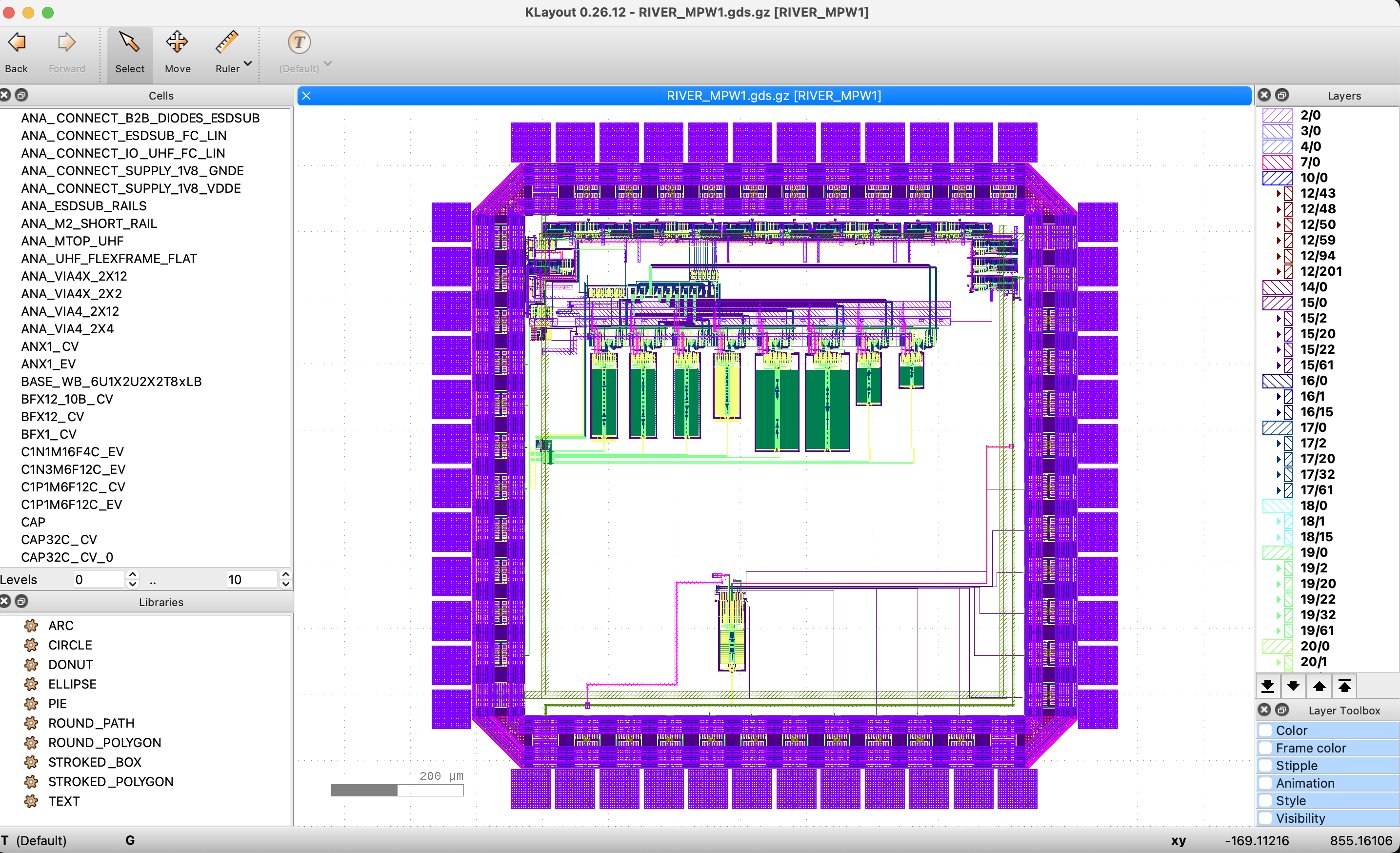
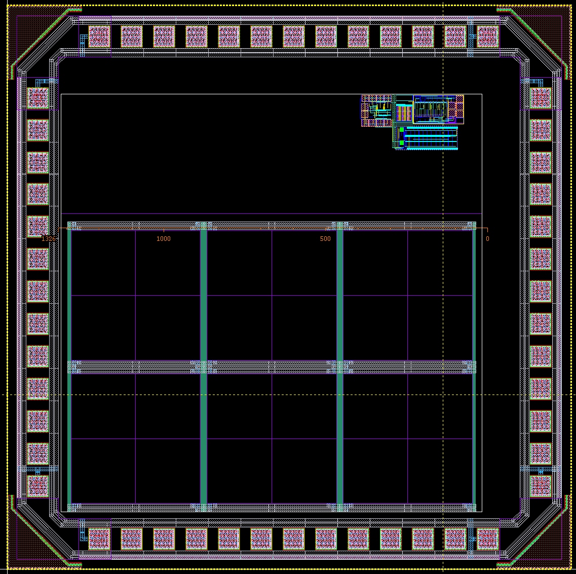
Layout
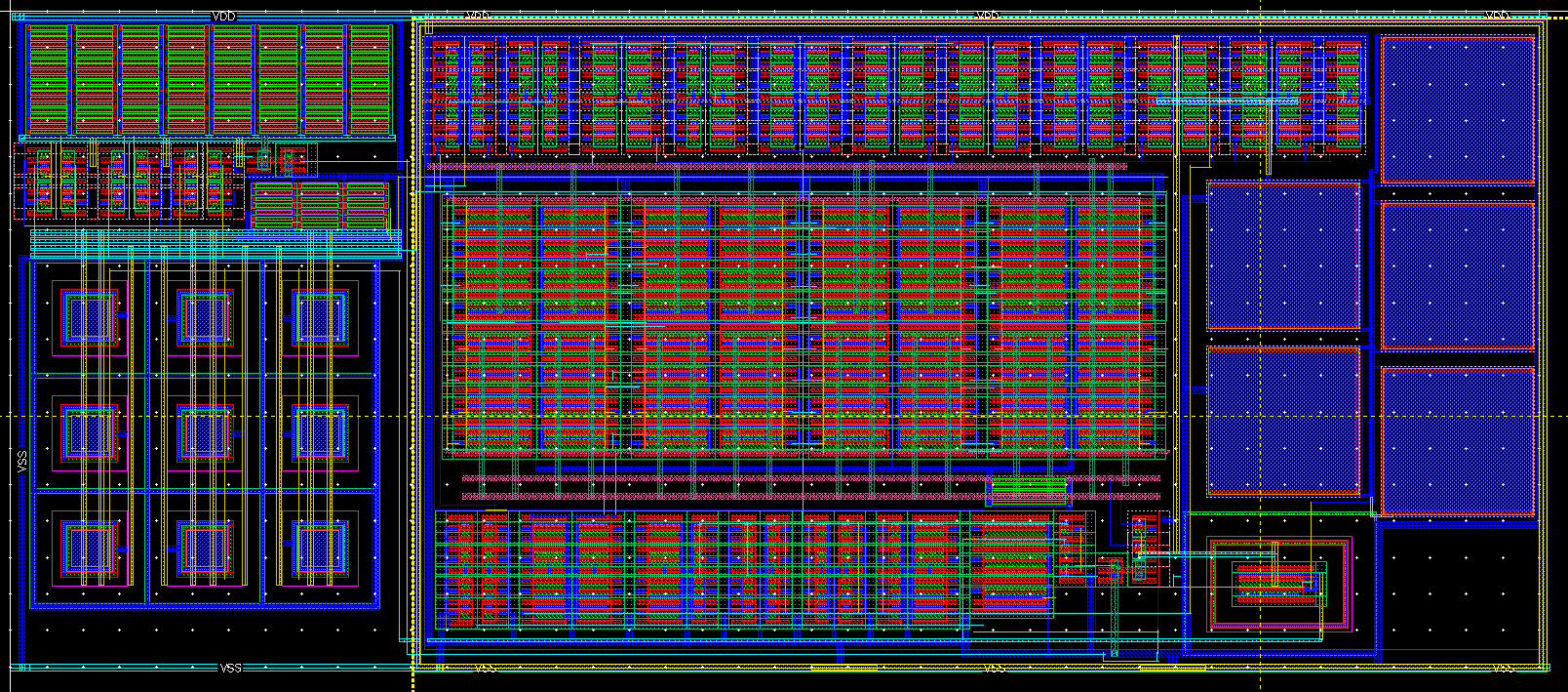
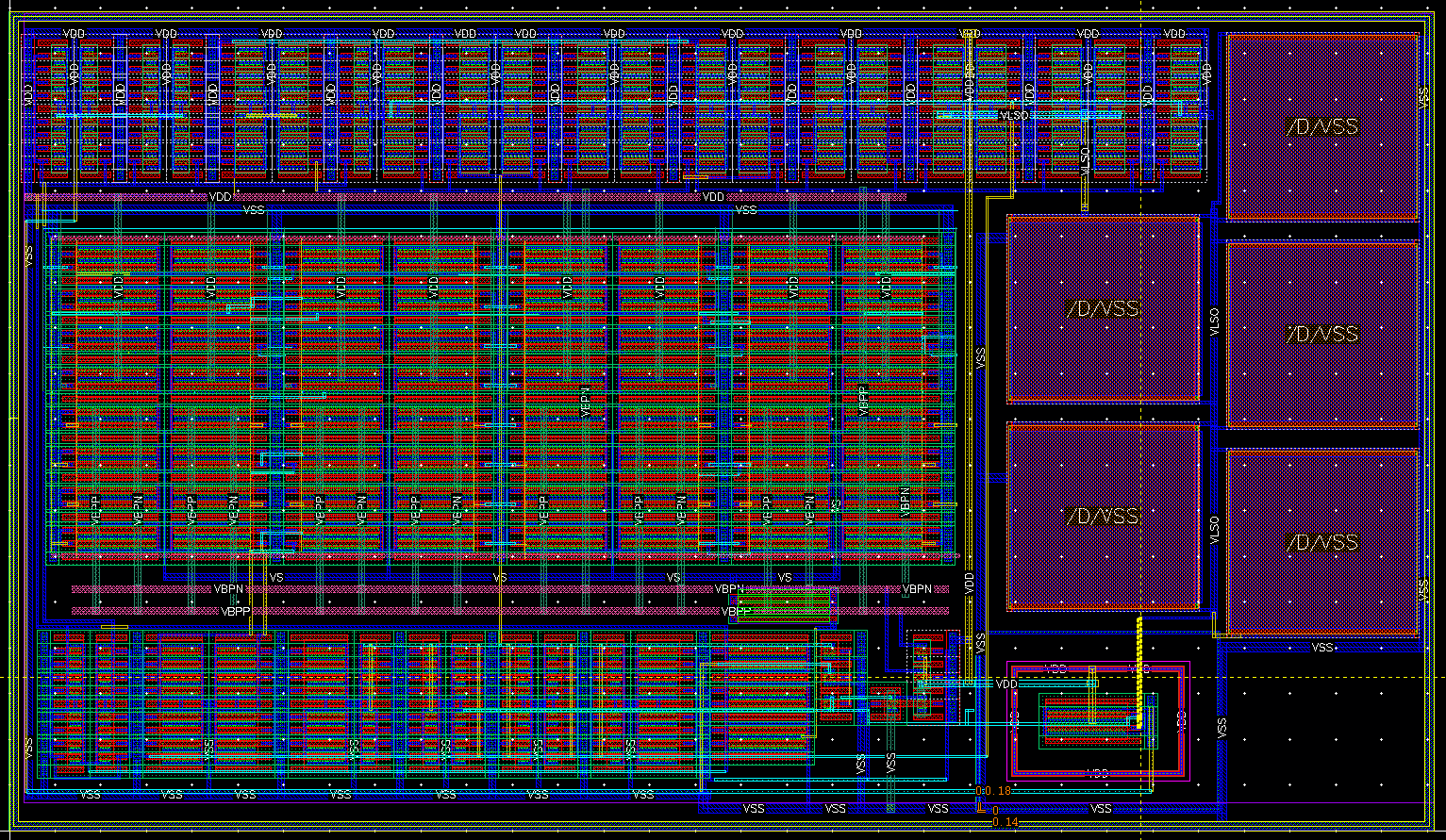
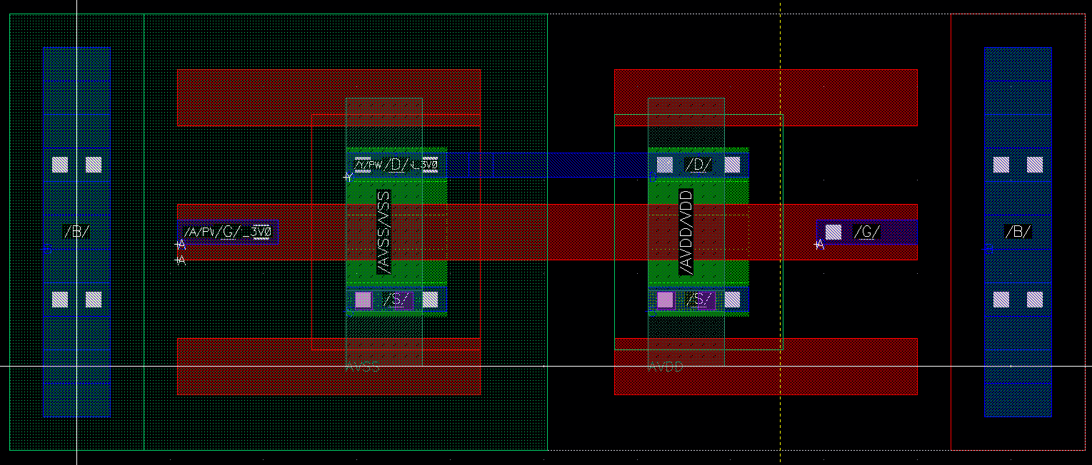
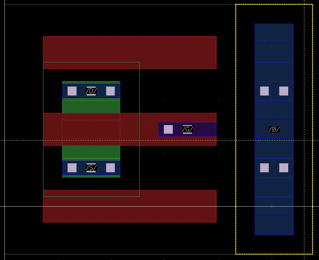
Design
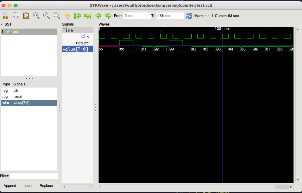
module counter(out, clk, reset);

  parameter WIDTH = 8;

  output [WIDTH-1 : 0] out;
  input 	       clk, reset;

  reg [WIDTH-1 : 0]   out;
  wire 	       clk, reset;

  always @(posedge clk or posedge reset)
    if (reset)
      out <= 0;
    else
      out <= out + 1;

endmodule // counter
https://github.com/wulffern/dicex/tree/main/sim/verilog/counter
/* Generated by Yosys 0.9 (git sha1 1979e0b) */

(* dynports =  1  *)
(* top =  1  *)
(* src = "counter.v:1" *)
module counter(out, clk, reset);
  (* src = "counter.v:11" *)
  wire [7:0] _00_;
...
  input reset;
  NOT _51_ (
    .A(_43_),
    .Y(_09_)
  );
...
  DFFSR _92_ (
    .C(clk),
    .D(_00_[7]),
    .Q(out[7]),
    .R(reset),
    .S(1'h0)
  );
  assign _43_ = out[0];
  assign _44_ = out[1];
  assign _45_ = out[2];
  assign _00_[2] = _11_;
  assign _46_ = out[3];
  assign _00_[3] = _12_;
  assign _47_ = out[4];
  assign _00_[4] = _13_;
  assign _48_ = out[5];
  assign _00_[5] = _14_;
  assign _49_ = out[6];
  assign _00_[6] = _15_;
  assign _50_ = out[7];
  assign _00_[7] = _16_;
  assign _00_[0] = _09_;
  assign _00_[1] = _10_;
endmodule
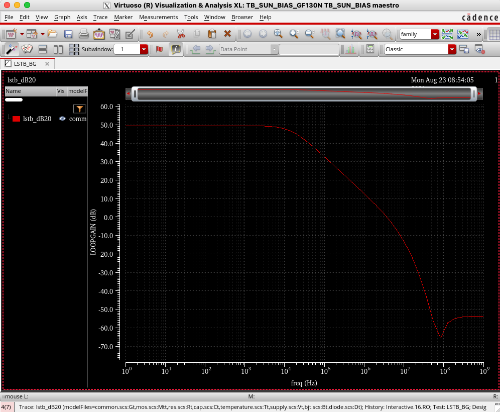
Simulation
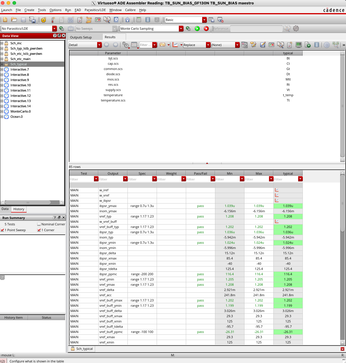
// Point Netlist Generated on: Aug 23 08:53:54 2021
// Generated for: spectre
// Design Netlist Generated on: Aug 23 08:53:53 2021
// Design library name: TB_SUN_BIAS_GF130N
// Design cell name: TB_SUN_BIAS
// Design view name: config
simulator lang=spectre
global 0
parameters t_pwrdwn=2 t_pwrup=1 pwrup=1 TFALL=100u TRISE=100u vdde=3.0
include "$PROJECT/lib/spectre/common.scs" section=Gt
include "$PROJECT/lib/spectre/mos.scs" section=Mtt
include "$PROJECT/lib/spectre/res.scs" section=Rt
include "$PROJECT/lib/spectre/cap.scs" section=Ct
include "$PROJECT/lib/spectre/temperature.scs" section=Tt
include "$PROJECT/lib/spectre/supply.scs" section=Vt
include "$PROJECT/lib/spectre/bjt.scs" section=Bt
include "$PROJECT/lib/spectre/diode.scs" section=Dt

// Inherited view list: spectre cmos_sch cmos.sch schematic veriloga ahdl
// pspice dspf
// Library name: SUN_BIAS_GF130N
// Cell name: SUN_BIAS
// View name: lpe_c_only_coupled
// View type: maskLayout
subckt SUN_BIAS IBPSR_1U\(25\) IBPSR_1U\(24\) IBPSR_1U\(23\) \
        IBPSR_1U\(22\) IBPSR_1U\(21\) IBPSR_1U\(20\) IBPSR_1U\(19\) \
        IBPSR_1U\(18\) IBPSR_1U\(17\) IBPSR_1U\(16\) IBPSR_1U\(15\) \
        IBPSR_1U\(14\) IBPSR_1U\(13\) IBPSR_1U\(12\) IBPSR_1U\(11\) \
        IBPSR_1U\(10\) IBPSR_1U\(9\) IBPSR_1U\(8\) IBPSR_1U\(7\) \
        IBPSR_1U\(6\) IBPSR_1U\(5\) IBPSR_1U\(4\) IBPSR_1U\(3\) \
        IBPSR_1U\(2\) IBPSR_1U\(1\) IBPSR_1U\(0\) PWRUP_3V0 VDD VFBI VFBO \
        VREF_1V2 VREF_BUFF_1V2 VREF_BUFF_1V2_FB VREF_FB VSS
        U1_VI\|R2 (U1_VI\|VS1 U1_VI\|53 VSS) ppolyf_u l=1e-05 w=5e-07 par=1 \
        s=1 m=1 dtemp=0
... (~ 8000 lines)

VVDD (VDD VSS) vsource dc=vdde type=pulse val0=0 val1=vdde period=5 \
        rise=TRISE fall=TFALL
V1 (PWRUP_3V0 VSS) vsource dc=pwrup*vdde type=pwl wave=[ 0 0 (t_pwrup) 0 \
        (t_pwrup + 1n) vdde (t_pwrdwn) vdde (t_pwrdwn + 1n) 0 ]
...
module counter(out, clk, reset);

  parameter WIDTH = 8;

  output [WIDTH-1 : 0] out;
  input 	       clk, reset;

  reg [WIDTH-1 : 0]   out;
  wire 	       clk, reset;

  always @(posedge clk or posedge reset)
    if (reset)
      out <= 0;
    else
      out <= out + 1;

endmodule // counter
Want to learn more?
Preview of Advanced Integrated Circuits