l14_speed
- TFE4152 - Lecture 14
- Speed
- Flip-flops and speed
- Timing analysis tools
- Every gate must be simulated to provide behavior over input transition and load capacitance
- All analog blocks must have associated liberty file to describe behavior and timing paths If you integrate analog into digital top flow
- Delay estimation
- Elmore Delay
- Delay components
TFE4152 - Lecture 14
Speed
Source
| Week | Book | Monday | Book | Friday |
|---|---|---|---|---|
| 34 | Introduction, what are we going to do in this course. Why do you need it? | WH 1 , WH 15 | Manufacturing of integrated circuits | |
| 35 | CJM 1.1 | pn Junctions | CJM 1.2 WH 1.3, 2.1-2.4 | Mosfet transistors |
| 36 | CJM 1.2 WH 1.3, 2.1-2.4 | Mosfet transistors | CJM 1.3 - 1.6 | Modeling and passive devices |
| 37 | Guest Lecture - Sony | CJM 3.1, 3.5, 3.6 | Current mirrors | |
| 38 | CJM 3.2, 3.3,3.4 3.7 | Amplifiers | CJM, CJM 2 WH 1.5 | SPICE simulation |
| 39 | Verilog | Verilog | ||
| 40 | WH 1.4 WH 2.5 | CMOS Logic | WH 3 | Speed |
| 41 | WH 4 | Q & A | WH 5 | Power/Wires |
| 42 | WH 6 | Scaling Reliability and Variability | WH 8 | Gates |
| 43 | WH 9 | Sequencing | WH 10 | Datapaths - Adders |
| 44 | WH 10 | Datapaths - Multipliers, Counters | WH 11 | Memories |
| 45 | WH 12 | Packaging | WH 14 | Test |
| 46 | Guest lecture - Nordic Semiconductor | |||
| 47 | CJM | Recap of CJM | WH | Recap of WH |
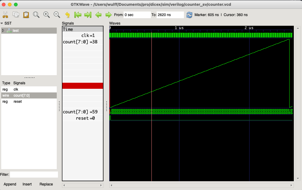
dicex/sim/verilog/counter_sv video on youtube https://youtu.be/dbt1aQsu_3I
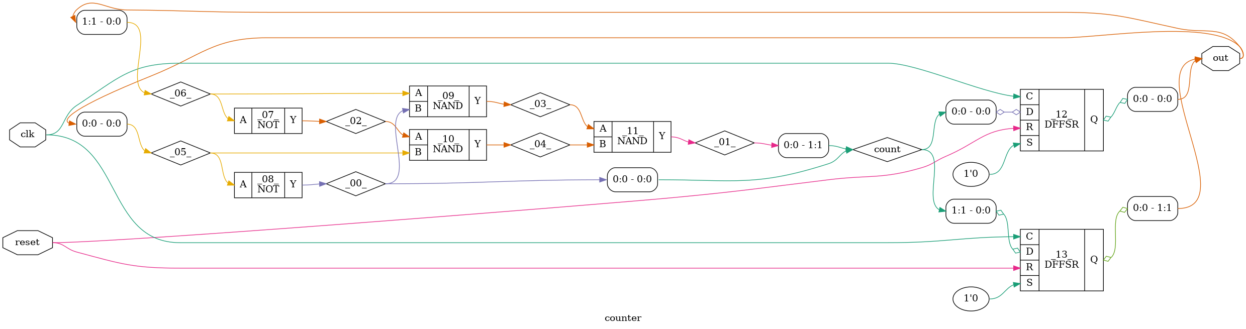
module counter(
               output logic [WIDTH-1:0] out,
               input logic              clk,
               input logic              reset
               );

   parameter WIDTH = 8;

   logic [WIDTH-1:0]                    count;
   always_comb begin
      count = out + 1;
   end

   always_ff @(posedge clk or posedge reset) begin
      if (reset)
        out <= 0;
      else
        out <= count;
   end

endmodule // counter
Speed
Why


Flip-flops and speed

dicex/lib/SUN_TR_GF130N.spi:

.SUBCKT DFRNQNX1_CV D CK RN Q QN AVDD AVSS
XA0 AVDD AVSS TAPCELLB_CV
XA1 CK RN CKN AVDD AVSS NDX1_CV
XA2 CKN CKB AVDD AVSS IVX1_CV
XA3 D CKN CKB A0 AVDD AVSS IVTRIX1_CV
XA4 A1 CKB CKN A0 AVDD AVSS IVTRIX1_CV
XA5 A0 A1 AVDD AVSS IVX1_CV
XA6 A1 CKB CKN QN AVDD AVSS IVTRIX1_CV
XA7 Q CKN CKB RN QN AVDD AVSS NDTRIX1_CV
XA8 QN Q AVDD AVSS IVX1_CV
.ENDS
Setup time: How long before clk does the data need to change

Hold time: How long after clk can the data change

Digital timing challenge: Estimate and analyze all delays over PVT
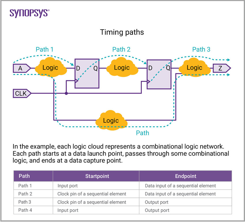
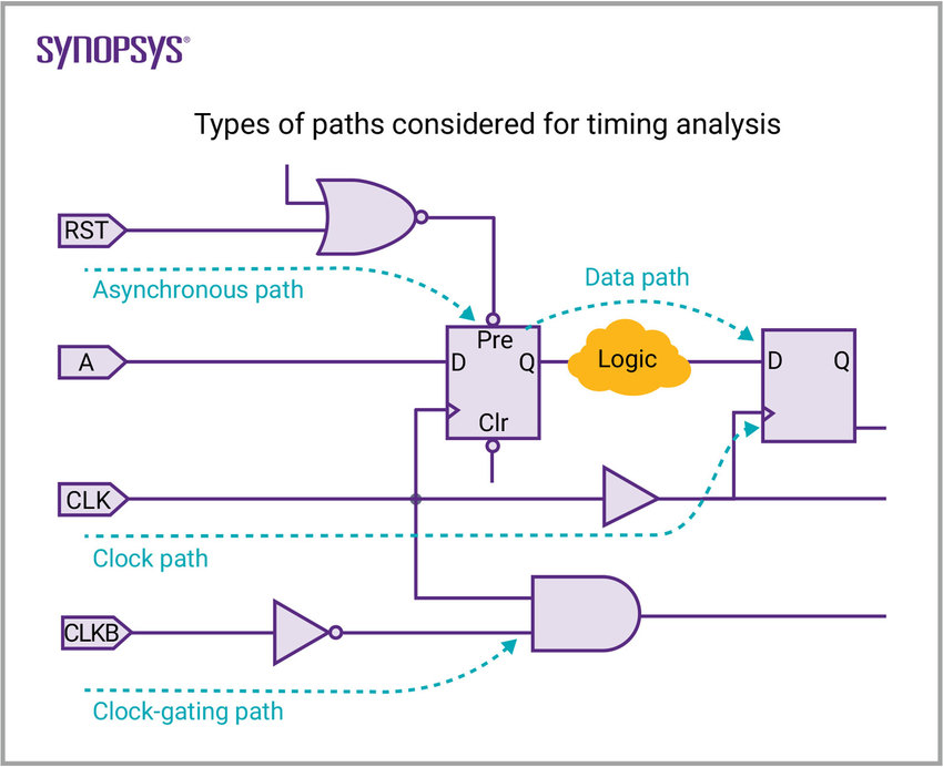
Timing analysis
Analyze arrival times of all nodes in a combinatorial circuit
\[arrival_j = max_{j \in fanin(i)}{arrival_j} + t_{pd_i} \Rightarrow a_j = max_{j \in fanin(i)}{a_j} + t_{pd_i}\] \[slack_i = required_i - arrival_j\]Positive slack (over PVT1) \(\Rightarrow\) Timing is OK Negative slack (over PVT1) \(\Rightarrow\) Timing is not OK

Timing analysis tools
Commercial Cadence Tempus
Free OpenTimer
What is timing analysis
What do the tools need?
Input and output delay paths as a function of input transition time and capacitive load, setup and hold time.
cell (INVX1) {
  cell_footprint : inv;
area : 16;
  cell_leakage_power : 0.0221741;
  pin(A)  {
    direction : input;
    capacitance : 0.00932456;
    rise_capacitance : 0.00932196;
    fall_capacitance : 0.00932456;
  }
  pin(Y)  {
    direction : output;
    capacitance : 0;
    rise_capacitance : 0;
    fall_capacitance : 0;
    max_capacitance : 0.503808;
    function : "(!A)";
    timing() {
      related_pin : "A";
      timing_sense : negative_unate;
      cell_fall(delay_template_5x5) {
        index_1 ("0.005, 0.0125, 0.025, 0.075, 0.15");
        index_2 ("0.06, 0.18, 0.42, 0.6, 1.2");
        values ( \
          "0.030906, 0.037434, 0.038584, 0.039088, 0.030318", \
          "0.04464, 0.057551, 0.073142, 0.077841, 0.081003", \
          "0.064368, 0.091076, 0.11557, 0.126352, 0.144944", \
          "0.139135, 0.174422, 0.232659, 0.261317, 0.321043", \
          "0.249412, 0.28434, 0.357694, 0.406534, 0.51187");
      }
      fall_transition(delay_template_5x5) {
        index_1 ("0.005, 0.0125, 0.025, 0.075, 0.15");
        index_2 ("0.06, 0.18, 0.42, 0.6, 1.2");
        values ( \
          "0.032269, 0.0648, 0.087, 0.1032, 0.1476", \
          "0.036025, 0.0726, 0.1044, 0.1236, 0.183", \
          "0.06, 0.0882, 0.1314, 0.1554, 0.2286", \
          "0.1494, 0.1578, 0.2124, 0.2508, 0.3528", \
          "0.288, 0.2892, 0.3192, 0.3576, 0.492");
      }
      cell_rise(delay_template_5x5) {
        index_1 ("0.005, 0.0125, 0.025, 0.075, 0.15");
        index_2 ("0.06, 0.18, 0.42, 0.6, 1.2");
        values ( \
          "0.037639, 0.056898, 0.083401, 0.104927, 0.156652", \
          "0.05258, 0.083003, 0.119028, 0.141927, 0.207952", \
          "0.07402, 0.112622, 0.162437, 0.191122, 0.271755", \
          "0.15767, 0.201007, 0.284096, 0.331746, 0.452958", \
          "0.285016, 0.326868, 0.415086, 0.481337, 0.653064");
      }
      rise_transition(delay_template_5x5) {
        index_1 ("0.005, 0.0125, 0.025, 0.075, 0.15");
        index_2 ("0.06, 0.18, 0.42, 0.6, 1.2");
        values ( \
          "0.031447, 0.059488, 0.0846, 0.0918, 0.138", \
          "0.047167, 0.0786, 0.1044, 0.1224, 0.1734", \
          "0.072, 0.096, 0.1398, 0.1578, 0.222", \
          "0.1866, 0.1914, 0.2358, 0.2748, 0.3696", \
          "0.3648, 0.3648, 0.384, 0.4146, 0.5388");
      }
    }
    internal_power() {
      related_pin : "A";
      fall_power(energy_template_5x5) {
        index_1 ("0.005, 0.0125, 0.025, 0.075, 0.15");
        index_2 ("0.06, 0.18, 0.42, 0.6, 1.2");
        values ( \
          "0.009213, 0.004772, 0.00823, 0.018532, 0.054083", \
          "0.009047, 0.005677, 0.005713, 0.015244, 0.049453", \
          "0.008669, 0.006332, 0.002998, 0.01159, 0.04368", \
          "0.007879, 0.007243, 0.001451, 0.004701, 0.030385", \
          "0.007605, 0.007297, 0.003652, 0.000737, 0.020842");
      }
      rise_power(energy_template_5x5) {
        index_1 ("0.005, 0.0125, 0.025, 0.075, 0.15");
        index_2 ("0.06, 0.18, 0.42, 0.6, 1.2");
        values ( \
          "0.023555, 0.029044, 0.041387, 0.051684, 0.087278", \
          "0.023165, 0.028621, 0.039211, 0.048916, 0.083039", \
          "0.023574, 0.02752, 0.036904, 0.045723, 0.077971", \
          "0.024479, 0.025247, 0.032268, 0.039242, 0.066587", \
          "0.024942, 0.025187, 0.029612, 0.034835, 0.057524");
      }
    }
  }
}
Every gate must be simulated to provide behavior over input transition and load capacitance
All analog blocks must have associated liberty file to describe behavior and timing paths If you integrate analog into digital top flow
Gate Delay
Delay definitions
| Parameter | Name | Description |
|---|---|---|
| t_pdr | max rising propagation delay | input to rising output cross 50 % |
| t_pdf | max falling propagation delay | input to falling output cross 50 % |
| t_pd | propagation delay | t_pdf = (t_pdr + t_pdf)/2 |
| t_r | rise time | 20 % to 80 % |
image ../ip/l14/delay_def.pdf removed
Delay definitions
| Parameter | Name| Description| | :– | :–| :–| | t_f | fall time | 80 % to 20 %| | t_cdr | min rising contamination delay | input to rising output cross 50 %| | t_cdf | min falling contamination delay | input to falling output cross 50 %| | t_cd | contamination delay | t_cd = (t_cdr + t_cdf)/2|
image ../ip/l14/delay_def.pdf removed
Delay estimation
How can we get a resonably accurate hand calculation model of delay?
\[C \approx 1 \text{ fF}/\mu\text{m}\] \[R \approx 1 \text{ k}\Omega\mu\text{m}\]image ../ip/l14/rc_pmos.pdf removed> image ../ip/l14/rc_nmos.pdf removed
Inverter with inverter load
\(C \approx 1 \text{ fF}/\mu\text{m}\), \(R \approx 1 \text{ k}\Omega\mu\text{m}\)
\[t_{pd} = R \times 6C = 6RC\] \[t_{pd} = 6 \times 1 \times 10^{3} \times 1 \times 10^{-15} \text{ s}\] \[t_{pd} = 6 \times 10^{-12} = 6 \text{ ps}\]image ../ip/l14/inv.pdf removed
It’s not a perfect model, but it’s good enough for hand calculation
Figure from Weste book
\[t_{pd} \approx \sum_{\text{nodes}}{R_{\text{nodes}-to-source} C_i}\] \[= R_1C_1 + (R_1 + R_2)C_2 + ... + (R_1 + R_2 + ... + R_N) C_N\]image ../ip/l14/rc_fit.pdf removed
Elmore Delay
Good enough for hand calculation
image ../ip/l14/elmore.pdf removed
Delay of 3-input NAND
image ../ip/l14/nand3.pdf removed
image ../ip/l14/nand.pdf removed image ../ip/l14/nand_tr.pdf removed
\[t_{pdr} = (9 + 5h)C\]image ../ip/l14/nand_pu.pdf removed
\[t_{pdf} = 3C\frac{R}{3} + 3C\frac{2R}{3} + (9 + 5h)C\frac{3R}{3}\] \[= (12 + 5h)RC\]image ../ip/l14/nand_pd.pdf removed Use Elmore
Assume \(h = 1\), \(RC \approx 1 \text{ ps}\)
Contamination delay
\[t_{cdr} = (9 + 5h)C\frac{R}{3} = (3 + \frac{5}{3}h)RC\] \[t_{cdr} = 4\frac{2}{3} \text{ ps}\]Propagation delay
\[t_{pdr} = (9 + 5h)RC = 14 \text{ ps}\] \[t_{pdf}= (12 + 5h)RC = 17 \text{ ps}\]Delay components
Parasitic delay (p)
p = 9 or 12 RC
Independent of load capacitance
Effort delay (f)
f = 5h RC
Proportional to load capacitance
Let’s use process independent unit \(d = \frac{d_{real}}{\tau}\), \(\tau = 3 RC\)
Parasitic delay \(\Rightarrow p = 12 RC / 3 RC = 4\)
Effort delay \(\Rightarrow f = 5h RC / 3RC = \frac{5}{3} h\)
Delay \(\Rightarrow d = f + p = \frac{5}{3}h + 4\)
Logical effort (g) is the ratio of the input capacitance of a gate to the input capacitance of an inverter delivering the same output current
image ../ip/l14/logical_effort.pdf removed
Parasitic delay \(\Rightarrow p = 4\)
Logic effort \(\Rightarrow g = \frac{5}{3}\)
Electrical effort \(\Rightarrow h = 1\)
Effort \(\Rightarrow f = gh\)
Delay \(\Rightarrow d = f + p = gh + p = 5\frac{2}{3}\)
Real delay \(\Rightarrow d = 5\frac{2}{3} \times 3 \text{ ps} = 17 \text{ ps}\)

Modern IC timing analysis requires computers with advanced programs2
Best number of stages
Which has shortest delay?

One stage \(f = 64 \Rightarrow D = 64 + 1 = 65\)
Three stage with \(f=4\) \(D_F = 12, p = 3 \Rightarrow D = 12 + 3 = 15\)
For close to optimal delay, use \(f = 4\) (Used to be \(f=e\))
Trends


Attack vector
module counter(
               output logic [WIDTH-1:0] out,
               input logic              clk,
               input logic              reset
               );

   parameter WIDTH = 8;

   logic [WIDTH-1:0]                    count;
   always_comb begin
      count = out + 1;
   end

   always_ff @(posedge clk or posedge reset) begin
      if (reset)
        out <= 0;
      else
        out <= count;
   end

endmodule // counter
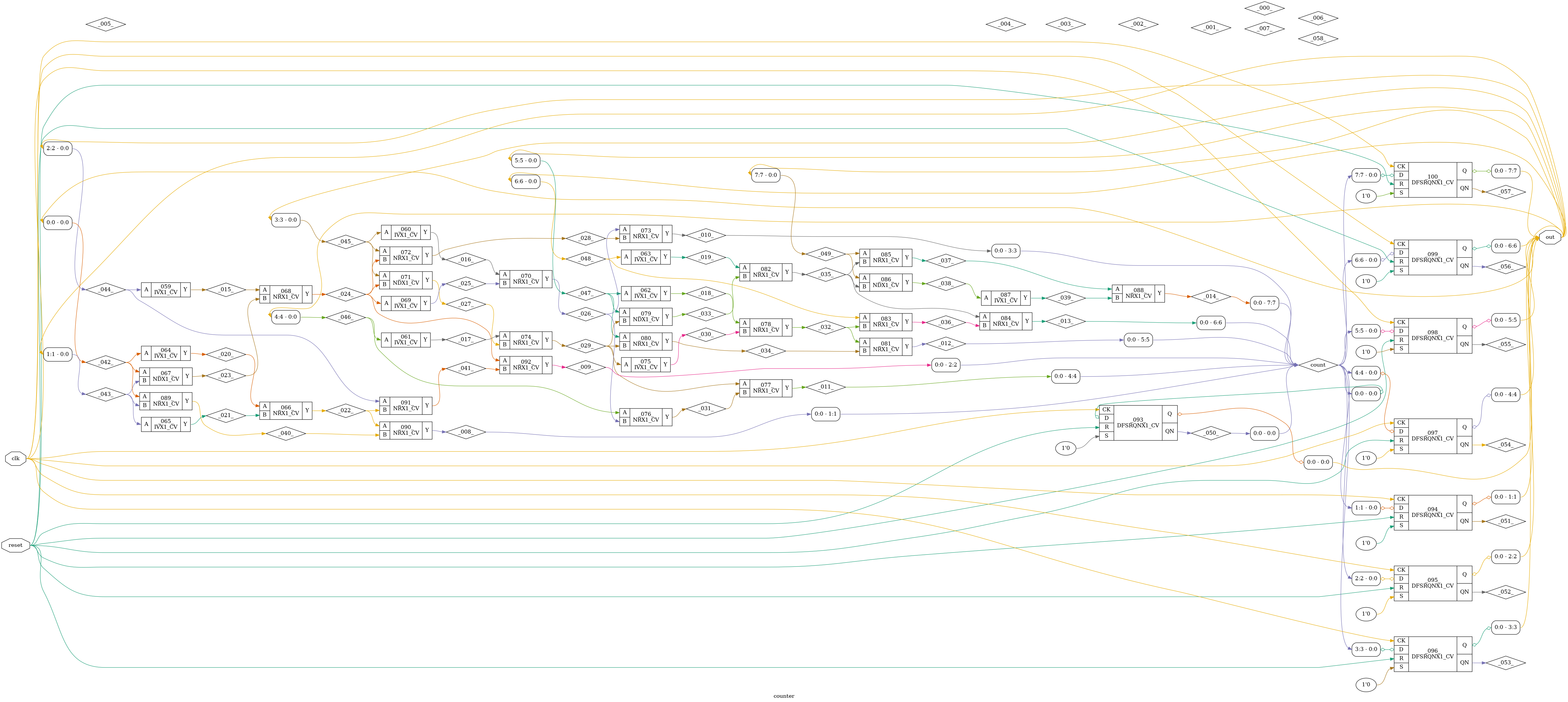
.SUBCKT counter out_7 out_6 out_5 out_4 out_3 out_2 out_1 out_0 clk reset AVDD AVSS
* SPICE netlist generated by Yosys 0_9 (git sha1 1979e0b1, gcc 10_3_0-1ubuntu1~20_10 -fPIC -Os)
X0 out_2 1 AVDD AVSS IVX1_CV
X1 out_3 2 AVDD AVSS IVX1_CV
X2 out_4 3 AVDD AVSS IVX1_CV
X3 out_5 4 AVDD AVSS IVX1_CV
X4 out_6 5 AVDD AVSS IVX1_CV
X5 out_0 6 AVDD AVSS IVX1_CV
X6 out_1 7 AVDD AVSS IVX1_CV
X7 6 7 8 AVDD AVSS NRX1_CV
X8 out_0 out_1 9 AVDD AVSS NDX1_CV
X9 1 9 10 AVDD AVSS NRX1_CV
X10 10 11 AVDD AVSS IVX1_CV
X11 2 11 12 AVDD AVSS NRX1_CV
X12 out_3 10 13 AVDD AVSS NDX1_CV
X13 out_3 10 14 AVDD AVSS NRX1_CV
X14 12 14 15 AVDD AVSS NRX1_CV
X15 3 13 16 AVDD AVSS NRX1_CV
X16 16 17 AVDD AVSS IVX1_CV
X17 out_4 12 18 AVDD AVSS NRX1_CV
X18 16 18 19 AVDD AVSS NRX1_CV
X19 4 17 20 AVDD AVSS NRX1_CV
X20 out_5 16 21 AVDD AVSS NDX1_CV
X21 out_5 16 22 AVDD AVSS NRX1_CV
X22 20 22 23 AVDD AVSS NRX1_CV
X23 5 21 24 AVDD AVSS NRX1_CV
X24 out_6 20 25 AVDD AVSS NRX1_CV
X25 24 25 26 AVDD AVSS NRX1_CV
X26 out_7 24 27 AVDD AVSS NRX1_CV
X27 out_7 24 28 AVDD AVSS NDX1_CV
X28 28 29 AVDD AVSS IVX1_CV
X29 27 29 30 AVDD AVSS NRX1_CV
X30 out_0 out_1 31 AVDD AVSS NRX1_CV
X31 8 31 32 AVDD AVSS NRX1_CV
X32 out_2 8 33 AVDD AVSS NRX1_CV
X33 10 33 34 AVDD AVSS NRX1_CV
X34 35 clk AVSS reset out_0 35 AVDD AVSS DFSRQNX1_CV
X35 32 clk AVSS reset out_1 36 AVDD AVSS DFSRQNX1_CV
X36 34 clk AVSS reset out_2 37 AVDD AVSS DFSRQNX1_CV
X37 15 clk AVSS reset out_3 38 AVDD AVSS DFSRQNX1_CV
X38 19 clk AVSS reset out_4 39 AVDD AVSS DFSRQNX1_CV
X39 23 clk AVSS reset out_5 40 AVDD AVSS DFSRQNX1_CV
X40 26 clk AVSS reset out_6 41 AVDD AVSS DFSRQNX1_CV
X41 30 clk AVSS reset out_7 42 AVDD AVSS DFSRQNX1_CV
V0 count_0 35 DC 0
V1 43 out_2 DC 0
V2 44 out_3 DC 0
V3 count_3 15 DC 0
V4 45 out_4 DC 0
V5 count_4 19 DC 0
V6 46 out_5 DC 0
V7 count_5 23 DC 0
V8 47 out_6 DC 0
V9 count_6 26 DC 0
V10 48 out_7 DC 0
V11 count_7 30 DC 0
V12 49 out_0 DC 0
V13 50 out_1 DC 0
V14 count_1 32 DC 0
V15 count_2 34 DC 0
.ENDS

dicex/sim/verilog/counter_sv/counter_attack_tb.cir
VDDA AVDD_ATTACK 0 dc 0.5 pulse(1.5 0.6 tcd trf trf tapw taper)