Lecture 11 - Analog SystemVerilog
If you find an error in what I’ve made, then fork, fix lectures/l11_aver.md, commit, push and create a pull request. That way, we use the global brain power most efficiently, and avoid multiple humans spending time on discovering the same error.
Design of integrated circuits is split in two, analog design, and digital design.
Digital design is highly automated. The digital functions are coded in SystemVerilog (yes, I know there are others, but don’t use those), translated into a gate level netlist, and automatically generated layout. Not everything is push-button automation, but most is.
Analog design, however, is manual work. We draw schematic, simulation with a mathematical model of the real world, draw the analog layout needed for the foundries to make the circuit, verify that we drew the schematic and layout the same, extract parasitics, simulate again, and in the end get a GDSII file.
When we mix analog and digital designs, we have two choices, analog on top, or digital on top.
In analog on top we take the digital IP, and do the top level layout by hand in analog tools.
In digital on top we include the analog IPs in the SystemVerilog, and allow the digital tools to do the layout. The digital layout is still orchestrated by people.
Which strategy is chosen depends on the complexity of the integrated circuit. For medium to low level of complexity, analog on top is fine. For high complexity ICs, then digital on top is the way to go.
Below is a description of the open source digital-on-top flow. The analog is included into GDSII at the OpenRoad stage of the flow.
The GDSII is not sufficient to integrate the analog IP. The digital needs to know how the analog works, what capacitance is on every digital input, the propagation delay for digital input to digital outputs , the relation between digital outputs and clock inputs, and the possible load on digital outputs.
The details on timing and capacitance is covered in a Liberty file. The behavior, or function of the analog circuit must be described in a SystemVerilog file.
But how do we describe an analog function in SystemVerilog? SystemVerilog is simulated in an digital simulator.

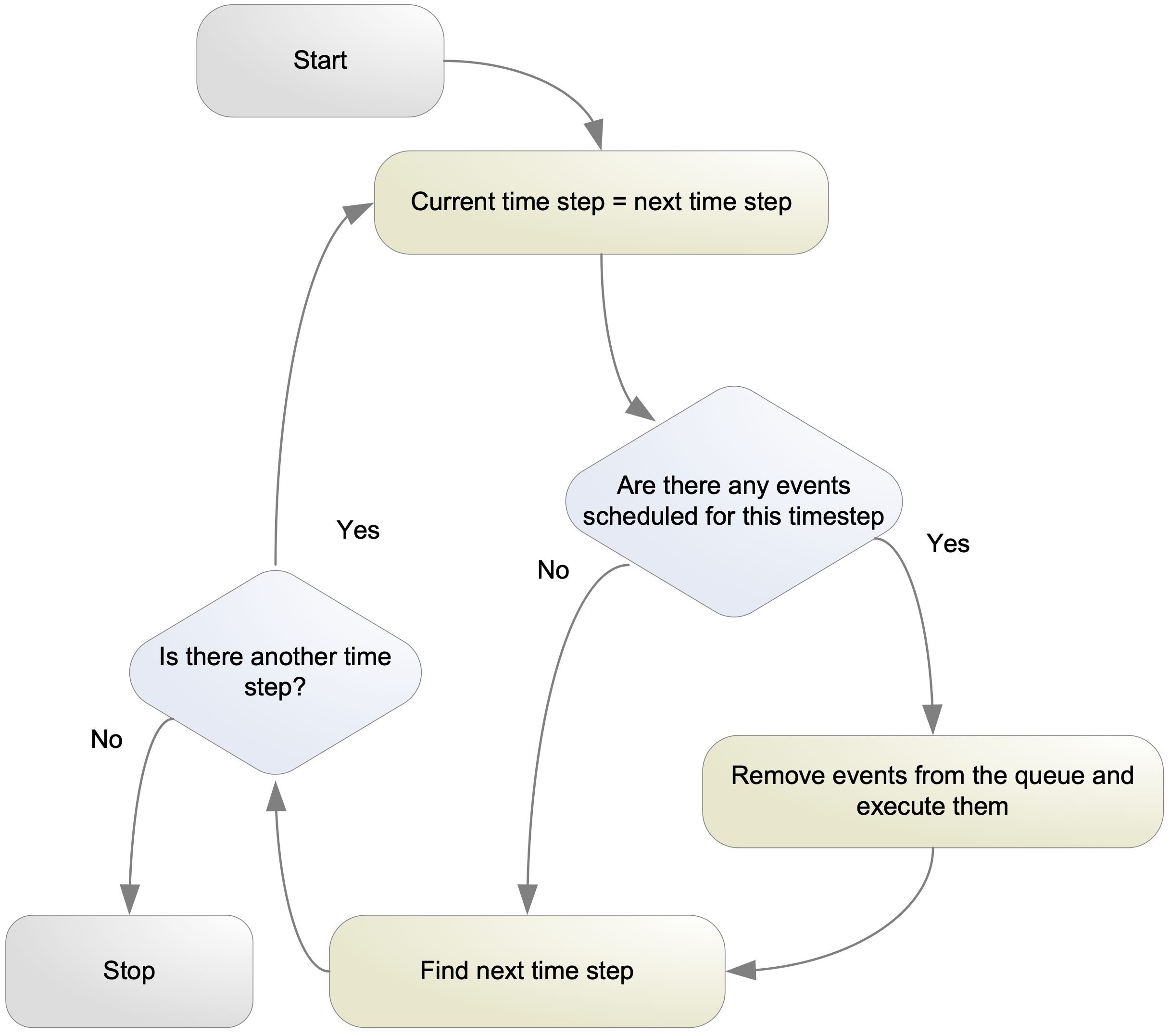
Digital simulation
Conceptually, the digital simulator is easy.
-
The order of execution of events at the same time-step do not matter
-
The system is causal. Changes in the future do not affect signals in the past or the now
In a digital simulator there will be an event queue, see below. From start, set the current time step equals to the next time step. Check if there are any events scheduled for the time step. Assume that execution of events will add new time steps. Check if there is another time step, and repeat.
Since the digital simulator only acts when something is supposed to be done, they are inherently fast, and can handle complex systems.
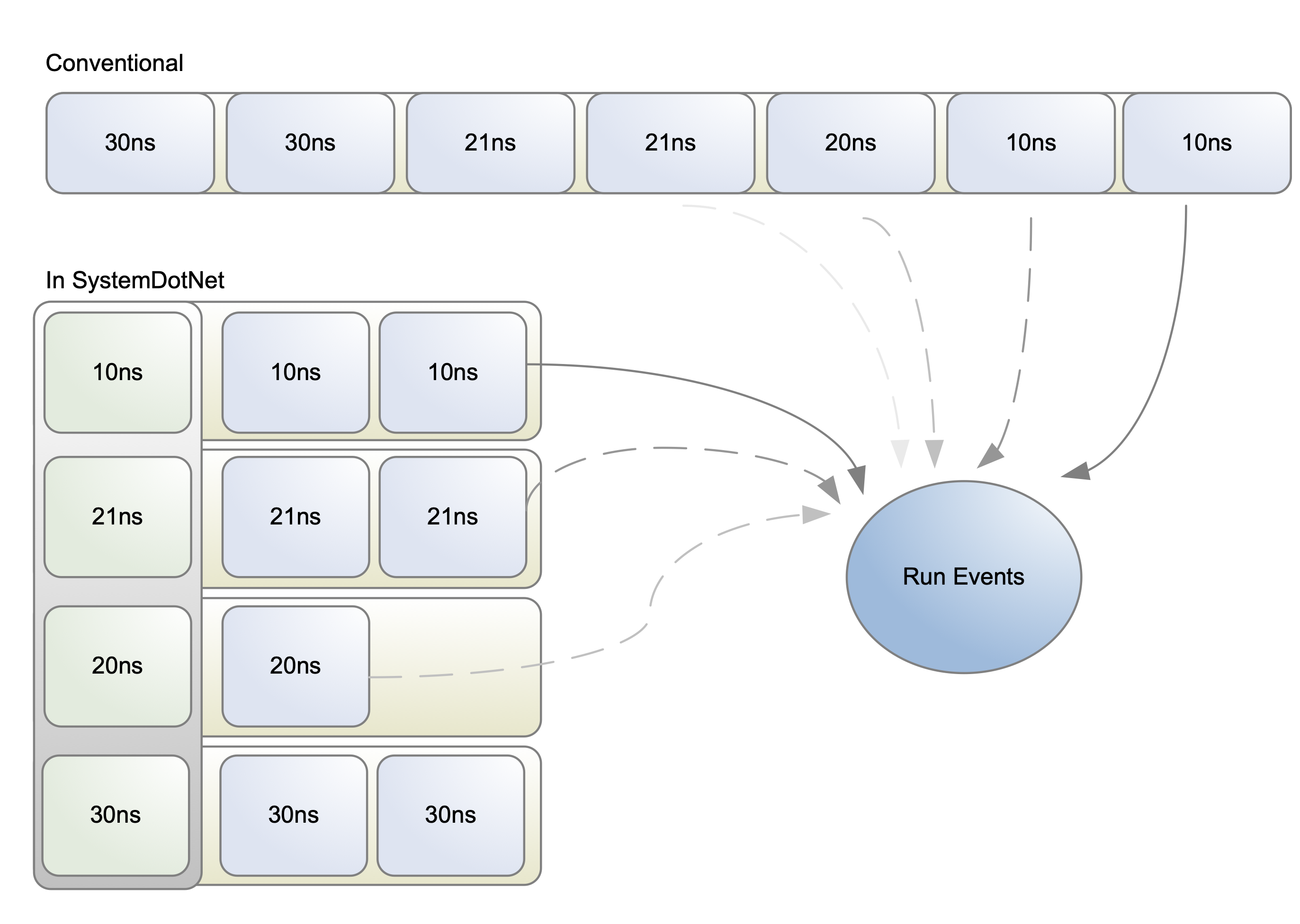
It’s a fun exercise to make a digital simulator. On my Ph.D I wanted to model ADCs, and first I had a look at SystemC, however, I disliked C++, so I made SystemDotNet
In SystemDotNet I implemented the event queue as a hash table, so it ran a bit faster. See below.
Digital Simulators
There are both commercial an open source tools for digital simulation. If you’ve never used a digital simulator, then I’d recommend you start with iverilog. I’ve made some examples at dicex.
Commercial
Open Source
Counter
Below is an example of a counter in SystemVerilog. The code can be found at counter_sv.
In the always_comb section we code what will become the combinatorial logic. In the always_ff section we code what will become our registers.
module counter(
               output logic [WIDTH-1:0] out,
               input logic              clk,
               input logic              reset
               );

   parameter WIDTH = 8;

   logic [WIDTH-1:0]                    count;
   always_comb begin
      count = out + 1;
   end

   always_ff @(posedge clk or posedge reset) begin
      if (reset)
        out <= 0;
      else
        out <= count;
   end

endmodule // counter
In the context of a digital simulator, we can think through how the event queue will look.
When the clk or reset changes from zero to 1, then schedule an event where if the reset is 1, then out will be zero in the next time step. If reset is 0, then out will be count in the next time step.
In a time-step where out changes, then schedule an event to set count to out plus one. As such, each positive edge of the clock at least 2 events must be scheduled in the register transfer level (RTL) simulation.
For example:
Assume `clk, reset, out = 0`

Assume event with `clk = 1`

0: Set `out = count` in next event (1)

1: Set `count = out + 1` using
   logic (may consume multiple events)

X: no further events
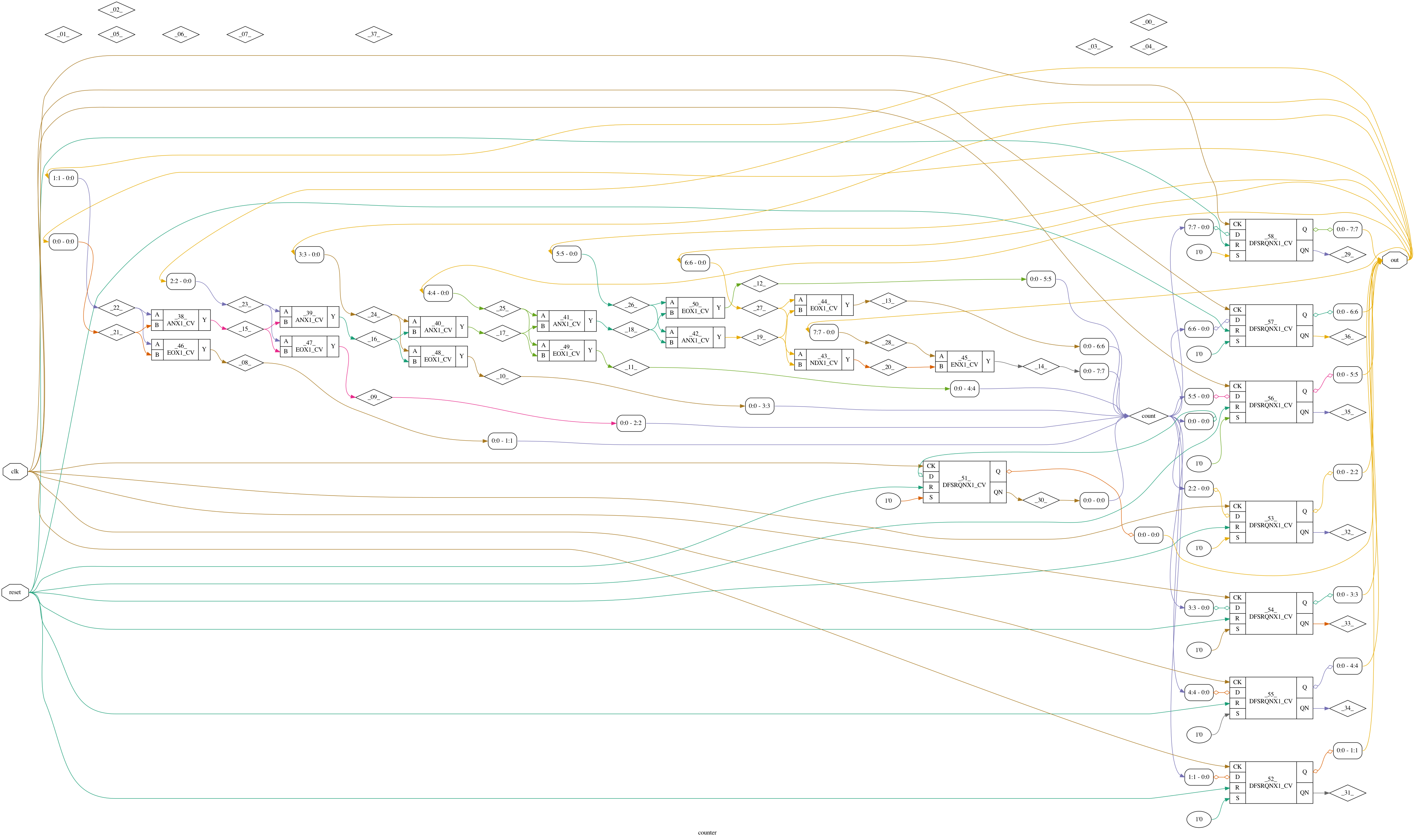
When we synthesis the code below into a netlist it’s a bit harder to see how the events will be scheduled, but we can notice that clk and reset are still inputs, and for example the clock is connected to d-flip-flops. The image below is the synthesized netlist
It should feel intuitive that a gate-level netlist will take longer to simulate than an RTL, there are more events.
Transient analog simulation
Analog simulation are different. There is no quantized time step. How fast “things” happen in the circuit is entirely determined by the time constants, change in voltage, and change in current in the system.
It is possible to have a fixed time-step in analog simulation, for example, we say that nothing is faster than 1 fs, so we pick that as our time step. If we wanted to simulate 1 s, however, that’s at least 1e15 events, and with 1 event per microsecond on a computer it’s still a simulation time of 31 years. Not a viable solution for all analog circuits.
Analog circuits are also non-linear, properties of resistors, capacitors, inductors, diodes may depend on the voltage or current across, or in, the device. Solving for all the non-linear differential equations is tricky.
An analog simulation engine must parse spice netlist, and setup partial/ordinary differential equations for node matrix
The nodal matrix could look like the matrix below, $i$ are the currents, $v$ the voltages, and $G$ the conductances between nodes.
\[\begin{pmatrix} G_{11} &G_{12} &\cdots &G_{1N} \\ G_{21} &G_{22} &\cdots &G_{2N} \\ \vdots &\vdots &\ddots & \vdots\\ G_{N1} &G_{N2} &\cdots &G_{NN} \end{pmatrix} \begin{pmatrix} v_1\\ v_2\\ \vdots\\ v_N \end{pmatrix}= \begin{pmatrix} i_1\\ i_2\\ \vdots\\ i_N \end{pmatrix}\]The simulator, and devices model the non-linear current/voltage behavior between all nodes
as such, the $G$’s may be non-linear functions, and include the $v$’s and $i$’s.
Transient analysis use numerical methods to compute time evolution
The time step is adjusted automatically, often by proprietary algorithms, to trade accuracy and simulation speed.
The numerical methods can be forward/backward Euler, or the others listed below.
If you wish to learn more, I would recommend starting with the original paper on analog transient analysis.
SPICE (Simulation Program with Integrated Circuit Emphasis) published in 1973 by Nagel and Pederson
The original paper has spawned a multitude of commercial, free and open source simulators, some are listed below.
If you have money, then buy Cadence Spectre. If you have no money, then start with ngspice.
Commercial
Free
Open Source
Mixed signal simulation
It is possible to co-simulate both analog and digital functions. An illustration is shown below.
The system will have two simulators, one analog, with transient simulation and differential equation solver, and a digital, with event queue.
Between the two simulators there would be analog-to-digital, and digital-to-analog converters.
To orchestrate the time between simulators there must be a global event and time-step control. Most often, the digital simulator will end up waiting for the analog simulator.
The challenge with mixed-mode simulation is that if the digital circuit becomes to large, and the digital simulation must wait for analog solver, then it does not work.
Most of the time, it’s stupid to try and simulate complex system-on-chip with mixed-signal , full detail, simulation.
For IPs, like an ADC, co-simulation works well, and is the best way to verify the digital and analog.
But if we can’t run mixed simulation, how do we verify analog with digital?

Analog SystemVerilog Example
The key idea is to model the analog behavior to sufficient detail such that we can verify the digital code. I think it’s best to have a look at a concrete example.
Take a high-speed camera IC, as illustrated below. Each pixel consists of a sensor, comparator and a memory, which are analog functions.
The control of each pixel, and the readout of each pixel is digital.
The image below is a model of the system in A 10 000 Frames/s CMOS Digital Pixel Sensor.
The principle of the paper is as follows:
- in each pixel, sample the output of the light sensor
- from top level, feed a digital ramp, and an analog ramp to all pixels at the same time
- in each pixel, use comparator to lock the memory when the analog ramp matches the sampled output from the sensor
As such, the complete image is converted from analog to digital in parallel.
![]()
The verilog below shows how the “Analog SystemVerilog” can be written.
In SystemVerilog there are “real” values for signals and values, or floating point.
The output of the sensor is modeled as the tmp variable. First tmp is reset to
v_erase on the ERASE` signal.
module PIXEL_SENSOR
  (
   input logic      VBN1,
   input logic      RAMP,
   input logic      RESET,
   input logic      ERASE,
   input logic      EXPOSE,
   input logic      READ,
   inout [7:0] DATA

   );

   real             v_erase = 1.2;
   real             lsb = v_erase/255;
   parameter real   dv_pixel = 0.5;

   real             tmp;
   logic            cmp;
   real             adc;

   logic [7:0]      p_data;

   //----------------------------------------------------------------
   // ERASE
   //----------------------------------------------------------------
   // Reset the pixel value on pixRst
   always @(ERASE) begin
      tmp = v_erase;
      p_data = 0;
      cmp  = 0;
      adc = 0;
   end
When EXPOSE is enabled to collect light, we reduce the tmp value proportional to an lsb and
a derivative dv_pixel. The dv_pixel is a parameter we can set on each pixel to model the
light.
The RAMP input signal is the analog ramp on the top level fed to each pixel. However,
since I did not have real wires in iverilog I had to be creative. Instead of a continuous
increasing value the RAMP is a clock that toggles 255 times. The actual “input” to the
ADC is the adc variable, but that is generated locally in each pixel. When the adc exceeds
the tmp we set cmp high.
The previous paragraph demonstrates an important point on analog systemVerilog models. They don’t need to be exact, and they don’t need to reflect exactly what happens in the “real world” of the analog circuit. What’s important is that the behavior from the outside resembles the real analog circuit, and that the digital designer makes the correct design choices.
The comparator locks the p_data, and, as we can see, the DATA is a tri-state bus that
is used both for reading and writing.
   //----------------------------------------------------------------
   // SENSOR
   //----------------------------------------------------------------
   // Use bias to provide a clock for integration when exposing
   always @(posedge VBN1) begin
      if(EXPOSE)
        tmp = tmp - dv_pixel*lsb;
   end

   //----------------------------------------------------------------
   // Comparator
   //----------------------------------------------------------------
   // Use ramp to provide a clock for ADC conversion, assume that ramp
   // and DATA are synchronous
   always @(posedge RAMP) begin
      adc = adc + lsb;
      if(adc > tmp)
        cmp <= 1;
   end

   //----------------------------------------------------------------
   // Memory latch
   //----------------------------------------------------------------
   always_comb  begin
      if(!cmp) begin
         p_data = DATA;
      end

   end

   //----------------------------------------------------------------
   // Readout
   //----------------------------------------------------------------
   // Assign data to bus when pixRead = 0
   assign DATA = READ ? p_data : 8'bZ;

endmodule // re_control
For more information on real-number modeling I would recommend The Evolution of Real Number Modeling