What I expect you to already know
If you find an error in what I’ve made, then fork, fix lectures/l01_need_to_know.md, commit, push and create a pull request. That way, we use the global brain power most efficiently, and avoid multiple humans spending time on discovering the same error.
- Quantum Mechanics
- Want to go deeper on the physics
- Silicon crystal
- Silicon crystal facts
- PN Junctions
- Computer models
- Built in voltage
- \(I_{diode} = I_s (e^{V_D/V_T} -1)\)
- Sesame
- Mosfets
- Drain Source Current (\(I_{DS}\))
- Large signal model
- Gate Source Voltage (\(V_{GS}\))
- Gate-source voltage
- Inversion level
- Weak inversion
- Moderate inversion
- Strong inversion
- The threshold voltage (\(V_{tn}\)) is defined as \(p_p = n_{ch}\)
- Drain-source voltage
- Strong inversion
- Low frequency model
- Intrinsic gain
- High frequency model
- \(C_{gs}\) and \(C_{gd}\)
- \(C_{sb}\) and \(C_{db}\)
- Weak inversion
- or subthreshold
- \(g_m/I_D\) or “bang for the buck”
- Velocity saturation
- What about holes (PMOS)
- OTHER
- As we make transistors smaller, we find new effects that matter, and that must be modelled.
- Drain induced barrier lowering (DIBL)
- Well Proximity Effect (WPE)
- Stress effects
- Gate current
- Hot carrier injection
- Channel initiated secondary-electron (CHISEL)
- Variability
- Provide \(I_2 = 1 \mu A\)
- Voltage variation
- Systematic variations
- Process variations
- Process corners
- Fix process variation
- Temperature variation
- It depends on \(V_{DD}\)
- How do we fix temperature variation?
- Random Variation
- Pelgrom’s law
- Transistors with same \(V_{GS}\)
- What else can we do?
- Transistor Noise
- Analog designer = Someone who knows how to deal with variation
- Current Mirrors
- Large signal vs small signal
- \(I \ne i\)
- \(V \ne v\)
- \(I = I_{bias} + i\)
- \(V = V_{bias} + v\)
- Current Mirror
- Amplifiers
- Source follower
- Source follower
- Common gate
- Common source
- Diff pairs are cool
- Operational transconductance amplifiers
- Digital
- \(SR\)-Latch
- \(SR\)-Latch
- D-Latch
- Digital can be synthesized in conductive peanut butter Barrie Gilbert?
- What about \(\text{Y} = \text{AB}\) and \(\text{Y} = \text{A} + \text{B}\)?
- \(\text{Y} = \text{AB} = \overline{\overline{\text{AB}}}\)
- \(\text{Y} = \text{A+B} = \overline{\overline{\text{A+B}}}\)
- AOI22: and or invert
- Tristate inverter
- Mux
- SystemVerilog
- There are other types of logic
- Elmore Delay
- Best number of stages
- Which has shortest delay?
- For close to optimal delay, use \(f = 4\) (Used to be \(f=e\))
- Pick two
- Power
- What is power?
- Power dissipated in a resistor
- Charging a capacitor to \(V_{DD}\)
- Energy to charge a capacitor to a voltage \(V_{DD}\)
- Discharging a capacitor to \(0\)
- Power consumption of digital circuits
- Sources of power dissipation in CMOS logic
- \(P_{switching}\) in logic gates
- Switching probability
- Strategies to reduce dynamic power
- IC Process
- Metal stack
- Metal routing rules on IC
- Lumped model
- Wire resistance
- Most wires: Copper
- Contacts
- Wire capacitance
- \(C_{total} = C_{top} + C_{bot} + 2C_{adj}\)
- Crosstalk
- FSM
- Mealy machine
- Moore machine
- Mealy versus Moore
There is quite few things I expect you to know something about. Below is an excerpt of the slideset from design of integrated circuits in 2021.
Quantum Mechanics
Want to go deeper on the physics

Classical equations
Kinetic energy + potential energy = Total Energy
\[\frac{1}{2 m} p^2 + V = E\]where \(p = m v\), \(m\) is the mass, \(v\) is the velocity and \(V\) is the potential
Quantum mechanical
State of a fermion is fully described by the probability amplitude \(\psi(x,t)\), also called the wave function of a particle.
The total energy of a particle is described by the Schrodinger Equation
\[\frac{1}{2 m} \frac{\hbar}{j^2} \frac{\partial^2}{\partial^2 x}\psi(x,t) + V(x)\psi(x,t) = -\frac{\hbar}{j}\frac{\partial}{\partial t} \psi(x,t)\]Quantum mechanics key concepts
To determine the moment or energy of multiple particles, you cannot consider them discrete entities. For example, the probabilty of finding a free electron in a particular location is given by
| $$P_1(x) = \int_{x_1}^{x_2} | \psi_1(x,0) | ^2\(, where\)P_1 = \int_{-\infty}^{\infty} | \psi_1(x,0) | = 1$$ |
| However, if we have two electrons, described by \(\psi_1(x,0)\) and \(\psi_2(x,0)\), then \(P_{12}(x) \ne P_1(x) + P_2(x)\), but rather $$P_{12}(x) = \int_{x_1}^{x_2} | \psi_1(x,0) + \psi_2(x,0) | ^2$$ |
It is the probability amplitudes that add, not the probabilities. And to make things more interesting, one solution to the Schrodinger equation is \(\psi(x,t) = Ae^{j(kx - \omega t)}\), where \(k\) is the wave number, and the \(\omega\) is the angular frequency. This is a complex function of position and time!
Silicon crystal
A pure silicon crystal can be visualized by a smallest repetable unit cell.
The unit cell is a face-centered cubic crystal with a lattice spacing of approx \(a = 5.43\)Å
- 8 corner atoms
- 6 face atoms
- 4 additional atoms spaced at 1/4 lattice spacing from 3 face atoms and 1 corner atom
Nearest neighbor \(d = \frac{1}{2}\left(a \sqrt{2}\right)\)

Energy levels of electrons in solids (current)
Electrons can only exist in discrete energy levels, given by the solutions to the Schrodinger equation. Since the probability amplitudes add for electrons in close proximity, then for crystals it’s more complicated.

Movement of electrons in solids
Electrons in solids can move if there are allowed energy states they can occupy.
In a semiconductor the valence band and first conduction band is separated by a band-gap (in conductors the bands overlap)
There are two options in semiconductors
- The valence band is not filled (holes), so electrons can move
- The electrons are given sufficient energy to reach conduction band, and are “free” to move
Silicon crystal facts
Although we know to an exterme precision exactly how electrons behave (Schrodinger equation). It is insainly complicated to compute the movement of electrons in a real silicon crystal with the Shrodinger equation.
Most “facts” about silicon crystal, like bandgap, effective mass, and mobility of electrons (or holes) are emprically determined.
In other words, we make assumptions, and grossly oversimplify, in order to handle complexity.
PN Junctions
\(q = 1.6 \times 10^{-19} [C]\) \(k = 1.38 \times 10^{-23} [J/K]\)
\[\mu_0 = \frac{2 \alpha}{q^2}\frac{h}{c} = 1.26 \times 10^{-6} [H/m]\] \[\epsilon_0 = \frac{1}{\mu_0 c^2} = 8.854 \times 10^{-12} [F/m]\]where q is unit charge, k is Boltzmann’s constant, h is Plancks constant, c is speed of light and alpha is the fine structure constant
Computer models
http://bsim.berkeley.edu/models/bsim4/
http://bsim.berkeley.edu/BSIM4/BSIM480.zip
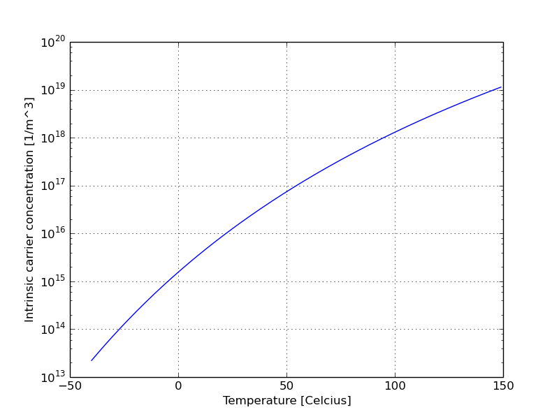
\(n_i \approx 1 \times 10^{16} [1/m^3] = 1 \times 10^{10} [1/cm^3]\) at 300 K
\[n_i^2 = n_0 p_0\] \[n_i = \sqrt{N_C N_V}e^{\frac{-E_g}{2kT}}\]\(N_C = 2\left(\frac{2 \pi m_{n}^* k T}{h^2}\right)^{3/2}\) \(N_V = 2\left(\frac{2 \pi m_{p}^* k T}{h^2}\right)^{3/2}\)
https://github.com/wulffern/dic2021/blob/main/2021-07-08_diodes/intrinsic.py
Solid state physics:
\[n_i = \sqrt{N_C N_V}e^{\frac{-E_g}{2kT}}\]BSIM 4.8, Intrinsic carrier concentration (page 122)
\[n_i = 1.45e10\frac{TNOM}{300.15}\sqrt{\frac{T}{300.15}}exp\left[21.5565981 - \frac{qE_g(TNOM)}{2 k_b T}\right]\]

Built in voltage
Comes from Fermi-Dirac statistics
\[\frac{n_n}{n_p} = \frac{e^{(E_{p} - \mu) / kT} + 1}{e^{(E_{n} - \mu) / kT} + 1} \approx e^{\frac{q \Phi_0}{kT}}\]where \(q \Phi_0\) is the energy (\(E_{p} - E_{n}\)) required to climb the potential barrier, \(kT\) is the thermal energy, \(\mu\) is the total chemical potential and \(n_n\) and \(n_p\) are the electron concentrations in the n-type and p-type.
\[\Phi_0 = V_T ln\left(\frac{N_A N_D}{n_i^2}\right)\] \[V_T = \frac{kT}{q}\]\(I_{diode} = I_s (e^{V_D/V_T} -1)\)
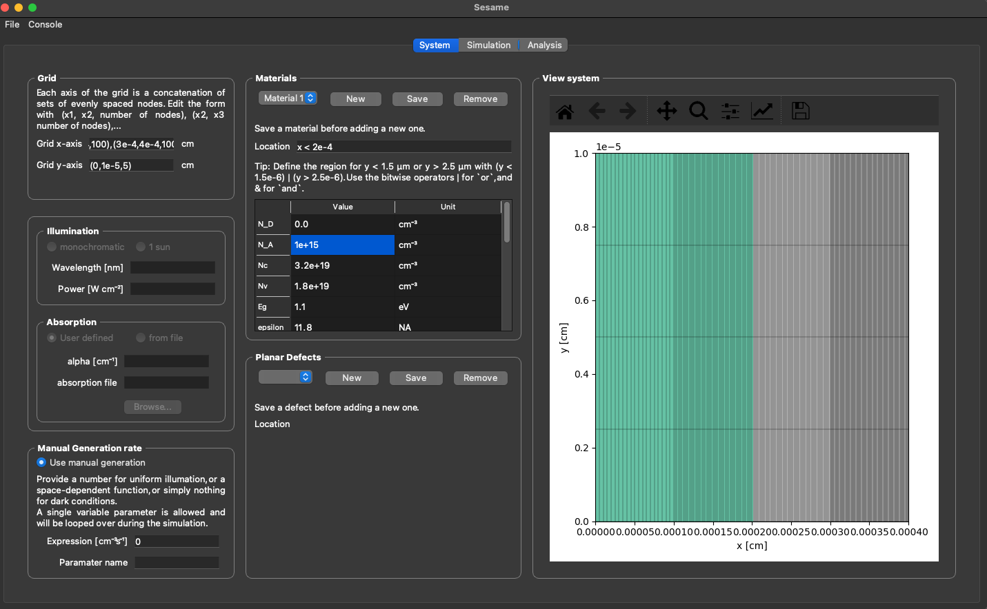
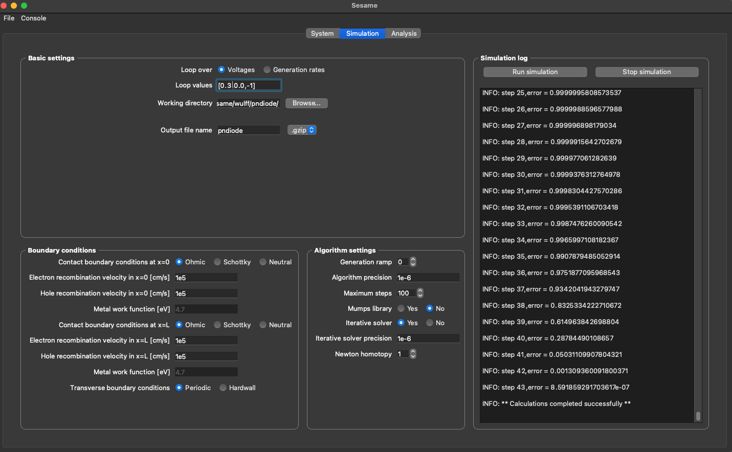
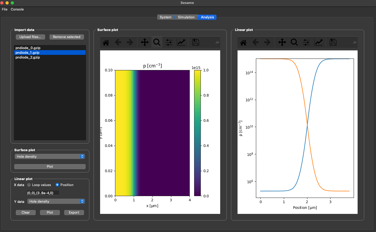
Sesame
Sesame is a Python3 package for solving the drift diffusion Poisson equations for multi-dimensional systems using finite differences.
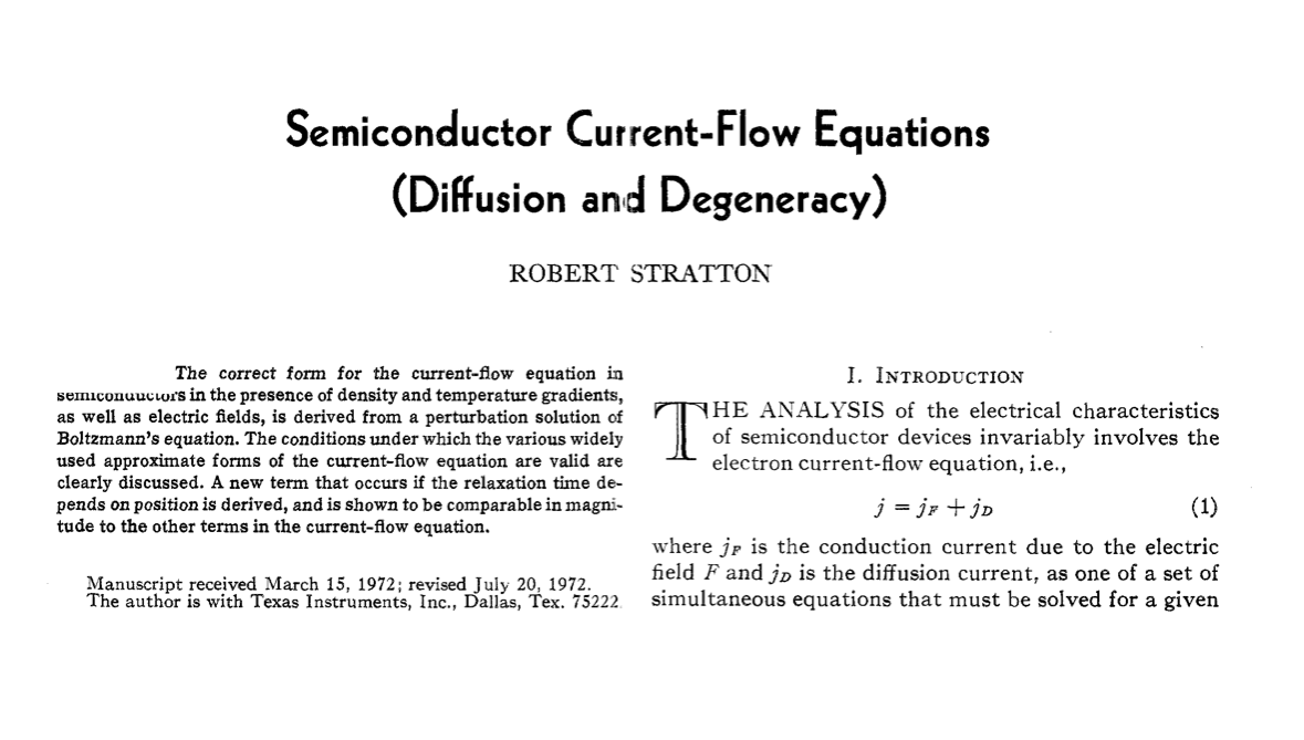
Semiconductor current-flow equations (diffusion and degeneracy), R.Stratton, IEEE Transactions on Electron Devices https://ieeexplore.ieee.org/document/1477063
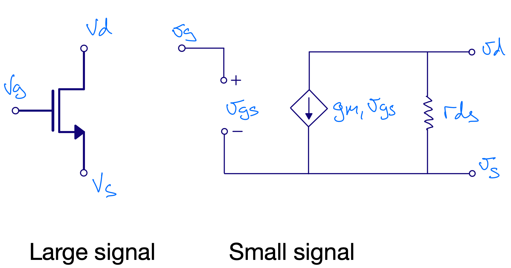
Mosfets
NMOS conduct for positive gate-to-source voltage

PMOS conduct for negative gate-to-source voltage


Drain Source Current (\(I_{DS}\))
dicex/sim/spice/NCHIO
Large signal model
\(I_{DS} = f(V_{GS},V_{DS},...)\)

Gate Source Voltage (\(V_{GS}\))
Gate-source voltage
| Param | Voltage [V] |
|---|---|
| VGS | 0 to 1.8 |
| VDS | 1.0 |
| VS | 0 |
| VB | 0 |

Inversion level
Define \(V_{eff} \equiv V_{GS} - V_{tn}\), where \(V_{tn}\) is the “threshold voltage”
| Veff | Inversion level |
|---|---|
| < 0 | weak inversion or subthreshold |
| 0 | moderate inversion |
| > 100 mV | strong inversion |
Weak inversion
The drain current is low, but not zero, when \(V_{eff} << 0\)
\[I_{DS} \approx I_{D0} \frac{W}{L} e^{V_{eff}/n V_{T}} \text{ if } V_{DS} > 3 V_{T}\] \[n \approx 1.5\]
Moderate inversion
Very useful region in real designs. Hard for hand-calculation. Trust the model.
Strong inversion
\[I_{DS} = \mu_n C_{ox} \frac{W}{L} \begin{cases} V_{eff} V_{DS} & \text{if }V_{DS} << V_{eff} \\[15pt] V_{eff} V_{DS} - V_{DS}^2/2 & \text{if } V_{DS} < V_{eff} \\[15pt] \frac{1}{2} V_{eff}^2 & \text{if } V_{DS} > V_{eff} \\[15pt] \end{cases}\]


The threshold voltage (\(V_{tn}\)) is defined as \(p_p = n_{ch}\)
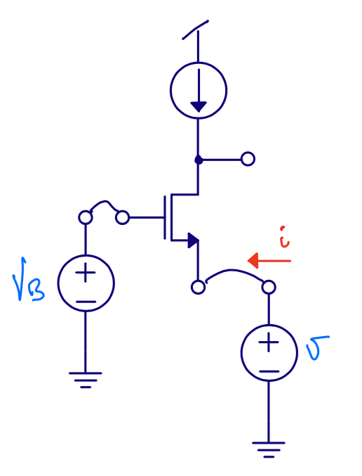
Drain-source voltage
| Param | Voltage [V] |
|---|---|
| VGS | 0.5 |
| VDS | 0 to 1.8 |
| VS | 0 |
| VB | 0 |

Strong inversion
\[I_{DS} = \mu_n C_{ox} \frac{W}{L} \begin{cases} V_{eff} V_{DS} & \text{if }V_{DS} << V_{eff} \\[15pt] V_{eff} V_{DS} - V_{DS}^2/2 & \text{if } V_{DS} < V_{eff} \\[15pt] \frac{1}{2} V_{eff}^2 & \text{if } V_{DS} > V_{eff} \\[15pt] \end{cases}\]


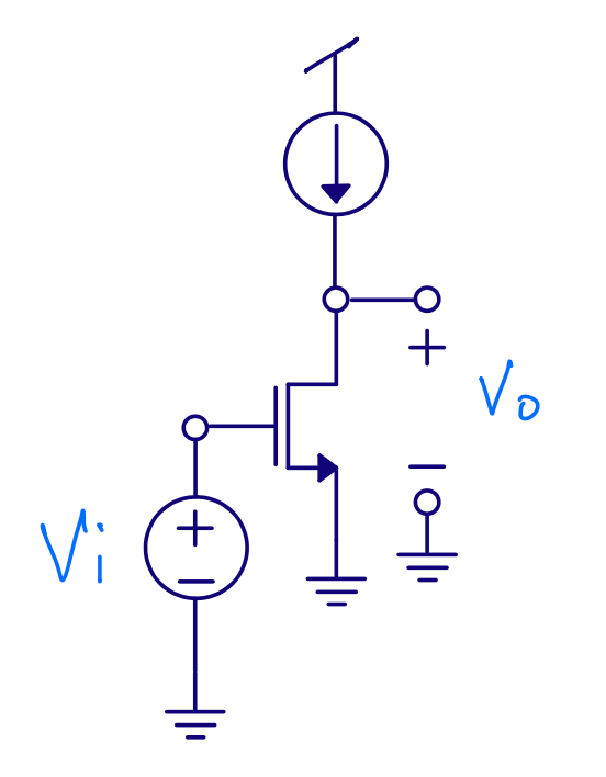
Low frequency model
\(g_{m} = \frac{\partial I_{DS}}{\partial V_{GS}}\\)
\(g_{ds} = \frac{1}{r_{ds}} = \frac{\partial I_{DS}}{\partial V_{DS}}\\)

Transconductance (\(g_m\))
Define \(\ell = \mu_n C_{ox} \frac{W}{L}\) and \(V_{eff} = V_{GS} - V_{tn}\)
\(I_{D} = \frac{1}{2} \ell (V_{eff})^2\) and \(V_{eff} = \sqrt{\frac{2I_{D}}{\ell}}\) and \(\ell = \frac{2I_D}{V_{eff}^2}\)
\[g_m = \frac{ \partial I_{DS}} {\partial V_{GS}} = \ell V_{eff} = \sqrt{2 \ell I_{D}}\] \[g_m = \ell V_{eff} = 2 \frac{I_D}{V_{eff}^2} V_{eff} = \frac{2 I_D}{V_{eff}}\]Define \(\ell = \mu_n C_{ox} \frac{W}{L}\) and \(V_{eff} = V_{GS} - V_{tn}\)
\[I_D = \frac{1}{2} \ell V_{eff}^2[1 + \lambda V_{DS} - \lambda V_{eff})]\] \[\frac{1}{r_{ds}} = g_{ds} = \frac{ \partial I_D}{\partial V_{DS} } = \lambda \frac{1}{2} \ell V_{eff}^2\]Assume channel length modulation is not there, then
\(I_D = \frac{1}{2} \ell V_{eff}^2\) which means \(\frac{1}{r_{ds}} = g_{ds} \approx \lambda I_D\)
Intrinsic gain
Define intrinsic gain as
\[A = \left|\frac{v_{out}}{v_{in}}\right| = g_m r_{ds} = \frac{g_m}{g_{ds}}\] \[A = \frac{2 I_D}{V_{eff}} \times \frac{1}{ \lambda I_D } = \frac{2}{\lambda V_{eff}}\]
vgaini = Gate Source Voltage = \(V_{eff} + V_{tn}\)

High frequency model


\(C_{gs}\) and \(C_{gd}\)
\[C_{gs} = \begin{cases} WLC_{ox} & \text{if }V_{DS} = 0 \\[15pt] \frac{2}{3}WLC_{ox} & \text{if }V_{DS} > V_{eff} \\[15pt] \end{cases}\] \[C_{gd} = C_{ox} W L_{ov}\]\(C_{sb}\) and \(C_{db}\)
Both are depletion capacitances
\[C_{sb} = (A_s + A_{ch}) C_{js}\] \[C_{js} = \frac{C_{j0}}{\sqrt{1 + \frac{V_{SB}}{\Phi_0}}}\] \[\Phi_0 = V_T ln\left(\frac{N_A N_D}{n_i^2}\right)\] \[C_{db} = A_d C_{jd}\] \[C_{js} = \frac{C_{j0}}{\sqrt{1 + \frac{V_{DB}}{\Phi_0}}}\]Be careful with \(C_{gd}\) (blame Miller)
If \(Y(s) = 1/sC\) then \(Y_1(s) = 1/sC_{in}\) and \(Y_2(s) = 1/sC_{out}\) where \(C_{in} = (1 + A) C\), \(C_{out} = (1 + \frac{1}{2})C\)
\[C_{1} = C_{gd} g_{m} r_{ds}\]\(C_{gd}\) can appear to be 10 to 100 times larger!
if gain from input to output is large

Weak inversion
or subthreshold
If \(V_{eff} < 0\) diffusion currents dominate.
\(I_{D} = I_{D0} \frac{W}{L} e^{V_eff / n V_T}\), where
\(V_T = kT/q\), \(n = (C_{ox} + C_{j0})/C_{ox}\)
\[I_{D0} = (n - 1) \mu_n C_{ox} V_T^2\] \[g_m = \frac{I_D}{nV_T}\]
\(g_m/I_D\) or “bang for the buck”
Subthreshold:
\[\frac{g_m}{I_D} = \frac{1}{nV_T} \approx 25.6 \text{ [S/A] @ 300 K}\]Strong inversion:
\[\frac{g_m}{I_D} = \frac{2}{V_{eff}}\]
Velocity saturation
Electron speed limit in silicon
\[v \approx 10^7 cm/s\] \[v = \mu_n E = \mu_n \frac{dV}{dx}\]\(\mu_n \approx 100 \text{ to } 600 \text{ } cm^2/Vs\) in nanoscale CMOS

Square law model
\[Q(x) = C_{ox}\left[V_{eff} - V(x)\right]\] \[v = \mu_n E = \mu_n \frac{dV}{dx}\] \[\ell = \mu_n C_{ox} \frac{W}{L}\] \[I_{D} = W Q(x) v = \ell L \left[ V_{eff} - V(x)\right] \frac{dV}{dx}\] \[I_{D} dx = \ell L \left[ V_{eff} - V(x)\right] dV\] \[I_{D} \int_0^L{dx} = \ell L \int_0^{V_{DS}}{\left[ V_{eff} - V(x)\right] dV}\] \[I_{D} \left[x\right]_0^L = \ell L \left[V_{eff}V - \frac{1}{2}V^2\right]_0^{V_{DS}}\] \[I_{D} L = \ell L \left[V_{eff}V_{DS} - \frac{1}{2} V_{DS}^2\right]\] \[@ V_{DS} = V_{eff} \Rightarrow I_{D} = \frac{1}{2} \ell V_{eff}^2\]Mobility Degredation
Multiple effects degrade mobility
- Velocity saturation
- Vertical fields reduce channel depth => more charge-carrier scattering
From square law \(g_{m} = \frac{\partial I_{D}}{\partial V_{GS}} = \ell V_{eff}\)
With mobility degredation \(g_{m(mob-deg)} = \frac{\ell}{2 \theta}\)
What about holes (PMOS)
In PMOS holes are the charge-carrier (electron movement in valence band)
\[\mu_p < \mu_n\]In intrinsic silicon: \(\mu_n \leq 1400 [cm^2/Vs] = 0.14 [m^2/Vs]\) \(\mu_p \leq 450 [cm^2/Vs] = 0.045 [m^2/Vs]\)
\[\mu_n \approx 3\mu_p\]\(v_{n\_max} \approx 2.3 \times 10^5 [m/s]\) \(v_{p\_max} \approx 1.6 \times 10^5 [m/s]\)
Doping (\(N_A \text{or} N_D\)) reduces \(\mu\)
OTHER
As we make transistors smaller, we find new effects that matter, and that must be modelled.
which is an opportunity for engineers to come up with cool names
https://ieeexplore.ieee.org/document/5247174

Drain induced barrier lowering (DIBL)

Well Proximity Effect (WPE)

Stress effects
| Stress | PMOS | NMOS |
|---|---|---|
| Stretch Fz | Good | Good |
| Compress Fy | OK | Good |
| Compress Fx | Good | Bad |
What can change stress?

Gate current

Hot carrier injection

Channel initiated secondary-electron (CHISEL)

Variability
Provide \(I_2 = 1 \mu A\)
Let’s use off-chip resistor \(R\), and pick \(R\) such that \(I_1 = 1 \mu A\)
Use \(\frac{W_1}{L_1} = \frac{W_2}{L_2}\)
What makes \(I_2 \ne 1 \mu A\)?

Voltage variation
Systematic variations
Process variations
Temperature variation
Random variations
Noise
Voltage variation
\[I_1 = \frac{V_{DD} - V_{GS1}}{R}\]If \(V_{DD}\) changes, then current changes.
Fix: Keep \(V_{DD}\) constant
Systematic variations
If \(V_{DS1} \ne V_{DS2} \rightarrow I_1 \ne I_2\)
If layout direction of \(M_1 \ne M_2 \rightarrow I_1 \ne I_2\)
If current direction of \(M_1 \ne M_2 \rightarrow I_1 \ne I_2\)
If \(V_{S1} \ne V_{S2} \rightarrow I_1 \ne I_2\)
If \(V_{B1} \ne V_{B2} \rightarrow I_1 \ne I_2\)
If \(WPE_{1} \ne WPE_{2} \rightarrow I_1 \ne I_2\)
If \(Stress_{1} \ne Stress_{2} \rightarrow I_1 \ne I_2\) …
Process variations
Assume strong inversion and active \(V_{eff} = \sqrt{\frac{2}{\mu_p C_{ox} \frac{W}{L}} I_1}\), \(V_{GS} = V_{eff} + V_{tp}\)
\[I_1 = \frac{V_{DD} - V_{GS}}{R} = \frac{V_{DD} - \sqrt{\frac{2}{\mu_p C_{ox} \frac{W}{L}} I_1} - V_{tp}}{R}\]\(\mu_p\), \(C_{ox}\), \(V_{tp}\) will all vary from die to die, and wafer lot to wafer lot.
Process corners
Common to use 5 corners, or Monte-Carlo process simulation
| Corner | NMOS | PMOS |
|---|---|---|
| Mtt | Typical | Typical |
| Mss | Slow | Slow |
| Mff | Fast | Fast |
| Msf | Slowish | Fastish |
| Mfs | Fastish | Slowish |
Fix process variation
Use calibration: measure error, tune circuit to fix error
For every single chip, measure voltage across known resistor \(R_1\) and tune \(R_{var}\) such that we get \(I_1 = 1 \mu A\)
Be careful with multimeters, they have finite input resistance (approximately 1 M\(\Omega\))

Temperature variation
Mobility decreases with temperature
Threshold voltage decreases with temperature.
\[I_D = \frac{1}{2}\mu_n C_{ox} (V_{GS} - V_{tn})^2\]High \(I_D =\) fast digital circuits
Low \(I_D =\) slow digital circuits
What is fast? High temperature or low temperature?
It depends on \(V_{DD}\)
Fast corner
- Mff (high mobility, low threshold voltage)
- High \(V_{DD}\)
- High or low temperature
Slow corner
- Mss (low mobility, high threshold voltage)
- Low \(V_{DD}\)
- High or low temperature
How do we fix temperature variation?
Accept it, or don’t use this circuit.
If you need stability over temperature, use 7.3.2 and 7.3.4 in CJM (SUN_BIAS_GF130N)
Random Variation
Mean \(\overline{x(t)} = \lim_{T\to\infty} \frac{1}{T}\int^{+T/2}_{-T/2}{ x(t) dt}\)
Mean Square \(\overline{x^2(t)} = \lim_{T\to\infty} \frac{1}{T}\int^{+T/2}_{-T/2}{ x^2(t) dt}\)
Variance \(\sigma^2 = \overline{x^2(t)} - \overline{x(t)}^2\)
where \(\sigma\) is the standard deviation. If mean is removed, or is zero, then \(\sigma^2 = \overline{x^2(t)}\)
Assume two random processes, \(x_1(t)\) and \(x_2(t)\) with mean of zero (or removed). \(x_{tot}(t) = x_1(t) + x_2(t)\) \(x_{tot}^2(t) = x_1^2(t) + x_2^2(t) + 2x_1(t)x_2(t)\)
Variance (assuming mean of zero) \(\sigma^2_{tot} = \lim_{T\to\infty} \frac{1}{T}\int^{+T/2}_{-T/2}{ x_{tot}^2(t) dt}\) \(\sigma^2_{tot} = \sigma_1^2 + \sigma_2^2 + \lim_{T\to\infty} \frac{1}{T}\int^{+T/2}_{-T/2}{ 2x_1(t)x_2(t) dt}\)
Assuming uncorrelated processes (covariance is zero), then \(\sigma^2_{tot} = \sigma_1^2 + \sigma_2^2\)
\(\ell = \mu_p C_{ox} \frac{W}{L}\) \(I_D = \frac{1}{2} \ell (V_{GS} - V_{tp})^2\)
Due to doping , length, width, \(C_{ox}\), \(V_{tp}\), … random varation
\[\ell_1 \ne \ell_2\] \[V_{tp1} \ne V_{tp2}\]As a result \(I_1 \ne I_2\), but we can make them close.
Pelgrom’s1 law
Given a random gaussian process parameter \(\Delta P\) with zero mean, the variance is given by
\[\sigma^2 (\Delta P) = \frac{A^2_P}{WL} + S_{P}^2 D^2\]where \(A_P\) and \(S_P\) are measured, and \(D\) is the distance between devices
Assume closely spaced devices (\(D \approx 0\)) \(\Rightarrow \sigma^2 (\Delta P) = \frac{A^2_P}{WL}\)
Transistors with same \(V_{GS}\)2
\[\frac{\sigma_{I_D}^2}{I_D^2} = \frac{1}{WL}\left[\left(\frac{gm}{I_D}\right)^2 \sigma_{vt}^2 + \frac{\sigma_{\ell}^2}{\ell}\right]\]Valid in weak, moderate and strong inversion
\(\frac{\sigma_{I_D}^2}{I_D^2} = \frac{1}{WL}\left[\left(\frac{gm}{I_D}\right)^2 \sigma_{vt}^2 + \frac{\sigma_{\ell}^2}{\ell}\right]\) \(\frac{\sigma_{I_D}}{I_D} \propto \frac{1}{\sqrt{WL}}\)
Assume \(\frac{\sigma_{I_D}}{I_D} = 10\%\), We want \(5\%\), how much do we need to change WL?
\[\frac{\frac{\sigma_{I_D}}{I_D}}{2} \propto \frac{1}{2\sqrt{WL}} = \frac{1}{\sqrt{4WL}}\]We must quadruple the area to half the standard deviation
\(1 \%\) would require 100 times the area
What else can we do?
\[\frac{\sigma_{I_D}^2}{I_D^2} = \frac{1}{WL}\left[\left(\frac{gm}{I_D}\right)^2 \sigma_{vt}^2 + \frac{\sigma_{\ell}^2}{\ell}\right]\]Strong inversion \(\Rightarrow \frac{gm}{I_D} = \frac{1}{2 V_{eff}} = low\)
Weak inversion \(\Rightarrow \frac{gm}{I_D} = \frac{q}{n k T} \approx 25\)
Current mirrors achieve best matching in strong inversion
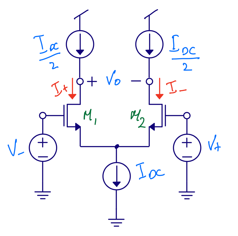
Offset voltage for a differential pair
\[i_o = i_{o+} - i_{o-} = g_m v_i = g_m (v_{i+} - v_{i-})\] \[\sigma_{v_i}^2 = \frac{\sigma_{I_D}^2}{gm^2} = \frac{1}{WL}\left[\sigma_{vt}^2 + \frac{I_D^2}{gm^2}\frac{\sigma_{\ell}^2}{\ell}\right]\]High \(\frac{gm}{I_D}\) is better (best in weak inversion)

Transistor Noise
Thermal noise Random scattering of carriers, generation-recombination in channel? \(PSD_{TH}(f) = \text{Constant}\)
Popcorn noise Carriers get “stuck” in oxide traps (dangling bonds) for a while. Can cause a short-lived (seconds to minutes) shift in threshold voltage \(PSD_{GR}(f) \propto \text{Lorentzian shape} \approx \frac{A}{1 + \frac{f^2}{f_0}}\)
Flicker noise Assume there are many sources of popcorn noise at different energy levels and time constants, then the sum of the spectral densities approaches flicker noise. \(PSD_{flicker}(f) \propto \frac{1}{f}\)

Analog designer = Someone who knows how to deal with variation
Current Mirrors


Large signal vs small signal
\(I \ne i\)
\(V \ne v\)
\(I = I_{bias} + i\)
\(V = V_{bias} + v\)
Current Mirror
\(M_1\) is diode connected (\(V_G = V_D\))

Amplifiers
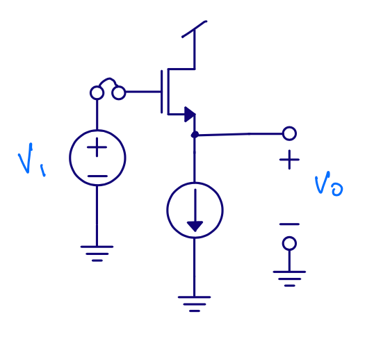
Source follower
Source follower
Input resistance \(\approx \infty\)
Gain \(A = \frac{v_o}{v_i}\)
Output resistance \(r_{out}\)
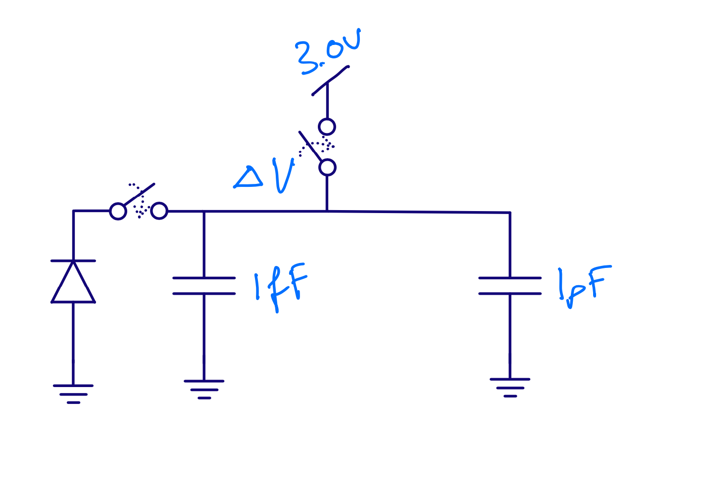
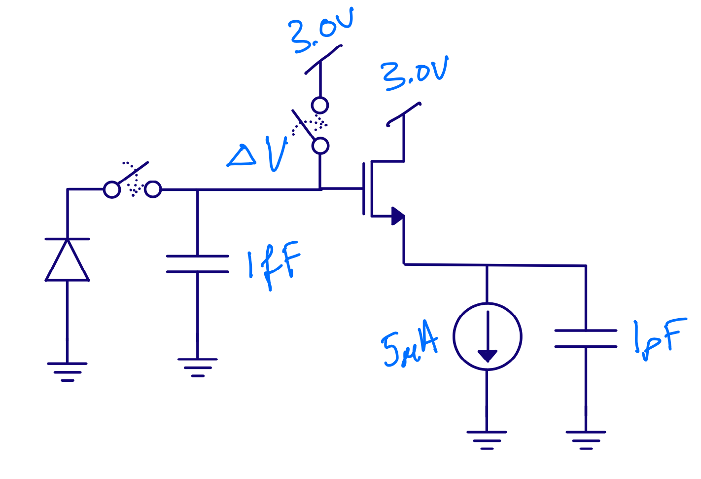
Assume 100 electrons
\[\Delta V = Q/C = -1.6 \times 10^{-19} \times 100 / (1\times 10^{-15}) = - 16\text{ mV}\]
Common gate
Input resistance \(r_{in} \approx \frac{1}{g_m}\left(1 + \frac{R_L}{r_{ds}}\right)\)
Gain \(\frac{v_o}{v_i} = 1 + g_m r_{ds}\)
Output resistance \(r_{out} = r_{ds}\)
Common source
Input resistance \(r_{in} \approx \infty\)
Output resistance \(r_{out} = r_{ds}\), it’s same circuit as the output of a current mirror
Gain \(\frac{v_o}{v_i} = - g_m r_{ds}\)
Diff pairs are cool
Can choose between
\[v_o = g_m r_{ds} v_i\]and
\[v_o = -g_m r_{ds} v_i\]by flipping input (or output) connections
Operational transconductance amplifiers
Digital
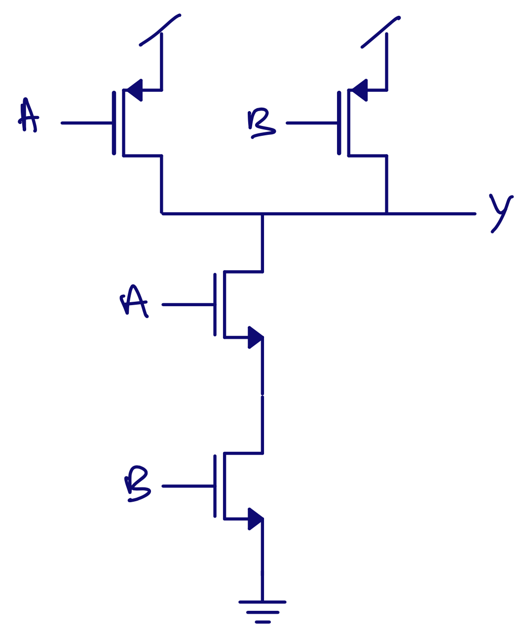
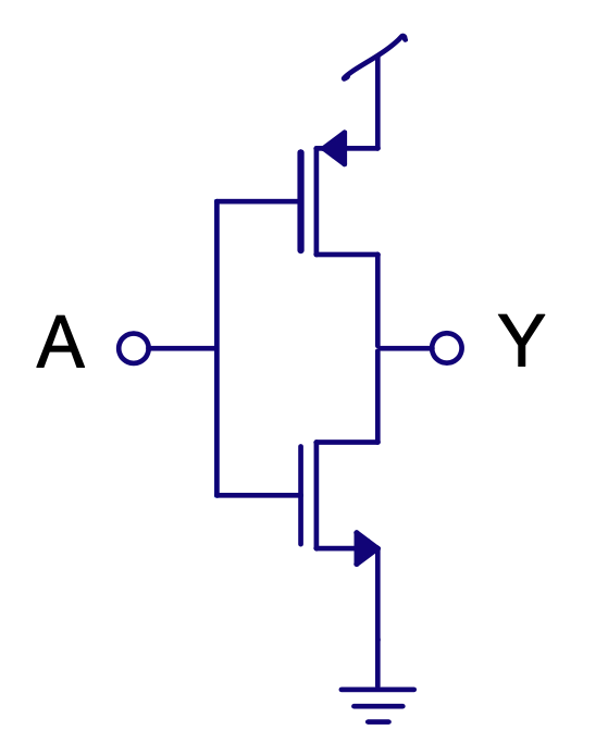
Rules for inverting static CMOS logic
Pull-up OR \(\Rightarrow\) PMOS in series \(\Rightarrow\) POS AND \(\Rightarrow\) PMOS in paralell \(\Rightarrow\) PAP
Postraumatic Papaya
Pull-down OR \(\Rightarrow\) NMOS in paralell \(\Rightarrow\) NOP AND \(\Rightarrow\) NMOS in series \(\Rightarrow\) NAS
[.table-separator: #000000, stroke-width(1)] [.table: margin(8)]
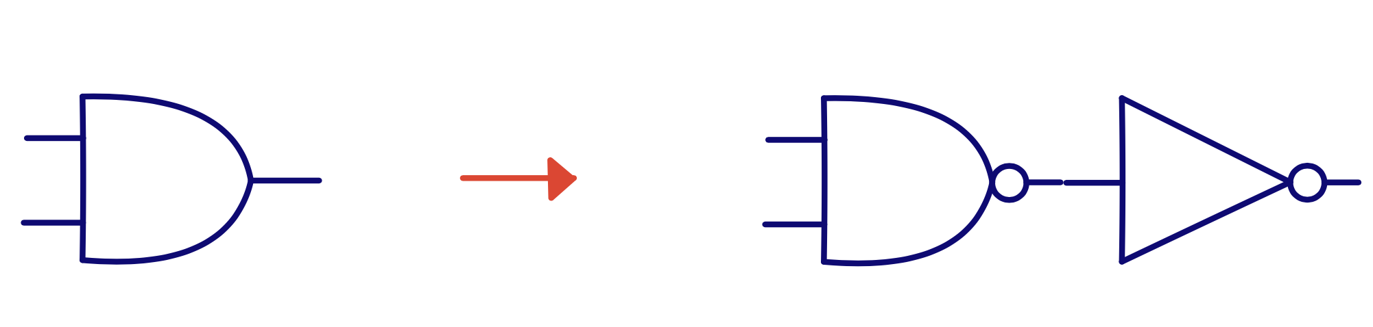
\(\text{Y} = \overline{\text{AB}} = \text{NOT ( A AND B)}\)
AND PU \(\Rightarrow\) PMOS in paralell PD \(\Rightarrow\) NMOS in series
Postraumatic Papaya
| A | B | NOT(A AND B) |
|---|---|---|
| 0 | 0 | 1 |
| 0 | 1 | 1 |
| 1 | 0 | 1 |
| 1 | 1 | 0 |
SUN_TR_GF130N
ssh://aurora/home/wulff/repos/sun_tr_gf130n.git
| Cell | Description |
|---|---|
| ANX1_CV | AND |
| BFX1_CV | Buffer |
| DFRNQNX1_CV | D Flip-flop with inverted output and inverted reset |
| IVTRIX1_CV | Tristate inverter, enable |
| IVX1_CV | Inverter |
| NDTRIX1_CV | Tristate NAND |
| NDX1_CV | NAND |
| NRX1_CV | NOR |
| ORX1_CV | OR |
| SCX1_CV | Schmitt-trigger |
| TAPCELLB_CV | Bulk connection |
| TIEH_CV | Tie high |
| TIEL_CV | Tie low |
\(SR\)-Latch
Use boolean expressions to figure out how gates work.
Remember De-Morgan
\(\overline{AB} = \overline{A}+ \overline{B}\) \(\overline{A+B} = \overline{A} \cdot \overline{B}\)
\[Q = \overline{R \overline{Q}} = \overline{R} + \overline{\overline{Q}} = \overline{R} + Q\] \[\overline{Q} = \overline{S Q} = \overline{S} + \overline{Q} = \overline{S} + \overline{Q}\]
\(SR\)-Latch
\(Q = \overline{R} + Q\), \(\overline{Q} =\overline{S} + \overline{Q}\)
| S | R | Q | ~Q |
|---|---|---|---|
| 0 | 0 | X | X |
| 0 | 1 | 0 | 1 |
| 1 | 0 | 1 | 0 |
| 1 | 1 | Q | ~Q |
D-Latch
| C | D | Q | ~Q |
|---|---|---|---|
| 0 | X | Q | ~Q |
| 1 | 0 | 0 | 1 |
| 1 | 1 | 1 | 0 |

Digital can be synthesized in conductive peanut butter Barrie Gilbert?
What about \(\text{Y} = \text{AB}\) and \(\text{Y} = \text{A} + \text{B}\)?
\(\text{Y} = \text{AB} = \overline{\overline{\text{AB}}}\)
Y = A AND B = NOT( NOT( A AND B ) )
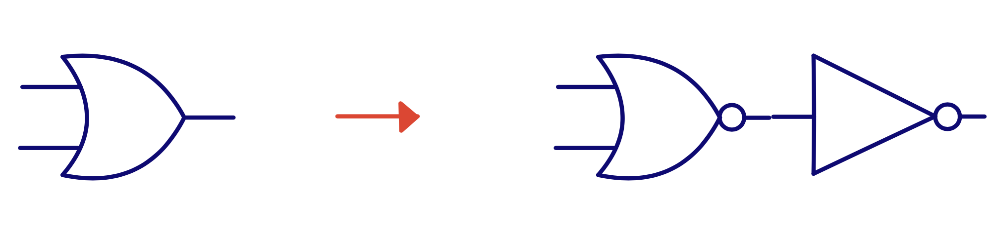
\(\text{Y} = \text{A+B} = \overline{\overline{\text{A+B}}}\)
Y = A OR B = NOT( NOT( A OR B ) )
AOI22: and or invert
Y = NOT( A AND B OR C AND D)
\[\text{Y} = \overline{\text{AB} + \text{CD}}\]
Postraumatic Papaya

[.table-separator: #000000, stroke-width(1)] [.table: margin(8)]
Tristate inverter
| E | A | Y |
|---|---|---|
| 0 | 0 | Z |
| 0 | 1 | Z |
| 1 | 0 | 1 |
| 1 | 1 | 0 |

[.table-separator: #000000, stroke-width(1)] [.table: margin(8)]
Mux
| S | Y |
|---|---|
| 0 | NOT(P1) |
| 1 | NOT(P0) |

D-Latch

D-Flip Flop


SystemVerilog
module counter(
               output logic [WIDTH-1:0] out,
               input logic              clk,
               input logic              reset
               );

   parameter WIDTH = 8;

   logic [WIDTH-1:0]                    count;
   always_comb begin
      count = out + 1;
   end

   always_ff @(posedge clk or posedge reset) begin
      if (reset)
        out <= 0;
      else
        out <= count;
   end

endmodule // counter
There are other types of logic
- True single phase clock (TSPC) logic
- Pass transistor logic
- Transmission gate logic
- Differential logic
- Dynamic logic
Consider other types of logic “rule breaking”, so you should know why you need it.

Dynamic logic => A Compiled 9-bit 20-MS/s 3.5-fJ/conv.step SAR ADC in 28-nm FDSOI for Bluetooth Low Energy Receivers
Elmore Delay
\[t_{pd} \approx \sum_{\text{nodes}}{R_{\text{nodes}-to-source} C_i}\] \[= R_1C_1 + (R_1 + R_2)C_2 + ... + (R_1 + R_2 + ... + R_N) C_N\]Good enough for hand calculation

Best number of stages
Which has shortest delay?


One stage \(f = 64 \Rightarrow D = 64 + 1 = 65\)
Three stage with \(f=4\) \(D_F = 12, p = 3 \Rightarrow D = 12 + 3 = 15\)
For close to optimal delay, use \(f = 4\) (Used to be \(f=e\))
Pick two

Power
What is power?
Instantanious power: \(P(t) = I(t)V(t)\)
Energy : \(\int_0^T{P(t)dt}\) [J]
Average power: \(\frac{1}{T} \int_0^T{P(t)dt}\) [W or J/s]
Power dissipated in a resistor
Ohm’s Law \(V_R = I_R R\)
\[P_R = V_R I_R = I_R^2 R = \frac{V_R^2}{R}\]Charging a capacitor to \(V_{DD}\)
Capacitor differential equation \(I_C = C\frac{dV}{dt}\)
\[E_{C} = \int_0^\infty{I_C V_C dt} = \int_0^\infty{ C \frac{dV}{dt} V_C dt} = \int_0^{V_C}{C V dV} = C\left[\frac{V^2}{2}\right]_0^{V_{DD}}\] \[E_{C} = \frac{1}{2} C V_{DD}^2\]Energy to charge a capacitor to a voltage \(V_{DD}\)
\[E_{C} = \frac{1}{2} C V_{DD}^2\] \[I_{VDD} = I_C = C \frac{dV}{dt}\] \[E_{VDD} = \int_0^\infty{I_{VDD} V_{DD} dt} = \int_0^\infty{C \frac{dV}{dt} V_{DD} dt} = C V_{DD}\int_0^{V_{DD}}{dV} = C V_{DD}^2\]Only half the energy is stored on the capacitor, the rest is dissipated in the PMOS
Discharging a capacitor to \(0\)
\[E_{C} = \frac{1}{2} C V_{DD}^2\]Voltage is pulled to ground, and the power is dissipated in the NMOS
Power consumption of digital circuits
\[E_{VDD} = C V_{DD}^2\]In a clock distribution network (chain of inverters), every output is charged once per clock cycle
\[P_{VDD} = C V_{DD}^2 f\]Sources of power dissipation in CMOS logic
\[P_{total} = P_{dynamic} + P_{static}\]Dynamic power dissipation
Charging and discharging load capacitances
short-circut current, when PMOS and NMOS conduct at the same time
\[P_{dynamic} = P_{switching} + P_{short circuit}\]Static power dissipation
Subthreshold leakage in OFF transistors
Gate leakage (tunneling current) through gate dielectric
Source/drain reverse bias PN junction leakage
\[P_{static} = \left( I_{sub} + I_{gate} + I_{pn} \right) V_{DD}\]\(P_{switching}\) in logic gates
Only output node transitions from low to high consume power from \(V_{DD}\)
Define \(P_i\) to be the probability that a node is 1
Define \(\overline{P_i} = 1 - P_i\) to be the probability that a node is 0
Define activity factor (\(\alpha_i\)) as the probability of switching a node from 0 to 1
If the probabilty is uncorrelated from cycle to cycle
\[\alpha_i = \overline{P_i}P_i\]Switching probability
Random data \(P = 0.5\), \(\alpha = 0.25\)
Clocks \(\alpha = 1\)

Strategies to reduce dynamic power
- Stop clock
- Stop activity
- Reduce clock frequency
- Turn off \(V_{DD}\)
- Reduce \(V_{DD}\)
Stop clock3

Stop activity

Reduce frequency

Turn off power supply 4

Reduce power supply (\(V_{DD}\))

IC Process
Metal stack
Often 5 - 10 layers of metal
| Metal | Material | Thickness | Purpose |
|---|---|---|---|
| Metal 1 - 2 | Copper | Thin | in gate routing |
| Metal 3-4 | Copper | Thicker | Between gates routing |
| Metal Z | Copper | Very thick | Cross chip routing. Local Power/Ground routing |
| Metal Y | Copper | Ultra thick | Cross chip power routing. Often used for RF inductors. |
| RDL | Aluminium | Ultra tick | Can tolerate high forces during wire bonding. |

Metal routing rules on IC
Odd numbers metals \(\Rightarrow\) Horizontal routing (as far as possible)
Even numbers metals \(\Rightarrow\) Vertical routing (as far as possible)
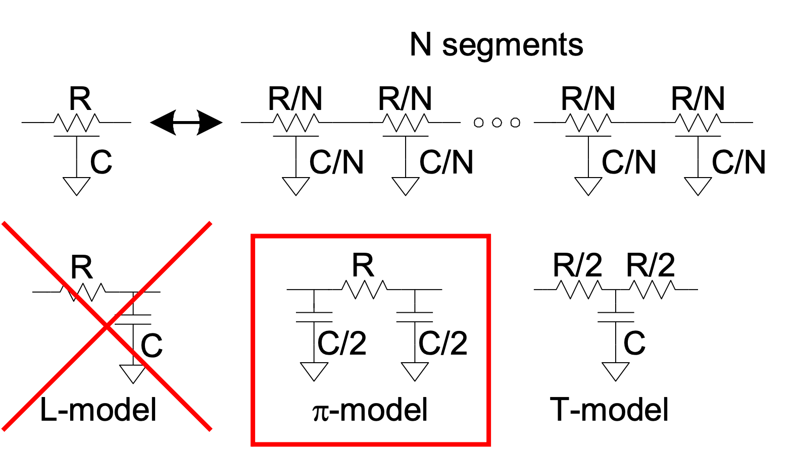
Lumped model
Use 1-segment \(\pi\)-model for Elmore delay
Wire resistance
resistivity \(\Rightarrow \rho\) [\(\Omega\)m]
\[R = \frac{\rho}{t}\frac{l}{w} = R_\square \frac{l}{w}\]\(R_\square\) = sheet resistance [\(\Omega/\square\)]
To find resistance, count the number of squares
\[R = R_\square \times \text{# of squares}\]Most wires: Copper
\(R_{sheet-m1} \approx \frac{1.7 \mu\Omega cm}{200 nm} \approx 0.1 \Omega/\square\)
\(R_{sheet-m9} \approx \frac{1.7 \mu\Omega cm}{3 \mu m} \approx 0.006 \Omega/\square\)
Pitfalls
Cu atoms diffuse into silicon and can cause damage
Must be surrounded by a diffusion barrier
Difficult high current densities (mA/\(\mu\)m) and high temperature (125 C)
Contacts
Contacts and vias can have 2-20 \(\Omega\)
Must use many contacts/vias for high current wires
Wire capacitance
\(C_{total} = C_{top} + C_{bot} + 2C_{adj}\)
Dense wires has about \(0.2 \text{ fF/}\mu\text{m}\)
Estimate delay of inverter driving a 1 mm long , 0.1 \(\mu m\) wide metal 1 wire with inverter load at the end
\(R_{sheet} = 0.1 \Omega/\square\) , \(R_{inv} = 1 k \Omega\), \(C_{w} = 0.2 fF/\mu m\), \(C_{inv} = 1 fF\)
Use Elmore \(t_{pd} = R_{inv}\frac{C_{wire}}{2} + (R_{wire} + R_{inv}) \left(\frac{C_{wire}}{2} + C_{inv}\right)\) \(= 1k \times 100f + (1k + 0.1 \times 1k/0.1)\times 101f = 0.3\text{ ns}\)

Crosstalk
A wire with high capacitance to a neighbor
An aggressor (0-1, 1-0) injects charge into neighbor wire
Increases delay
Noise on nonswitching wires

FSM
Mealy machine
An FSM where outputs depend on current state and inputs

Moore machine
An FSM where outputs depend on current state

Mealy versus Moore
| Parameter | Mealy | Moore |
|---|---|---|
| Outputs | depend on input and current state | output depend on current state |
| States | Same, or fewer states than Moore | |
| Inputs | React faster to inputs | Next clock cycle |
| Outputs | Can be asynchronous | Synchronous |
| States | Generally requires fewer states for synthesis | More states than Mealy |
| Counter | A counter is not a mealy machine | A counter is a Moore machine |
| Design | Can be tricky to design | Easy |
dicex/sim/counter_sv/counter.v
module counter(
               output logic [WIDTH-1:0] out,
               input logic              clk,
               input logic              reset
               );
   parameter WIDTH                      = 8;
   logic [WIDTH-1:0]                    count;

   always_comb begin
      count = out + 1;
   end

   always_ff @(posedge clk or posedge reset) begin
      if (reset)
        out <= 0;
      else
        out <= count;
   end

endmodule // counter

Battery charger FSM
Li-Ion batteries
Most Li-Ion batteries can tolerate 1 C during fast charge
For Biltema 18650 cells: \(1\text{ C} = 2950\text{ mA}\) \(0.1\text{ C} = 295\text{ mA}\)
Most Li-Ion need to be charged to a termination voltage of 4.2 V
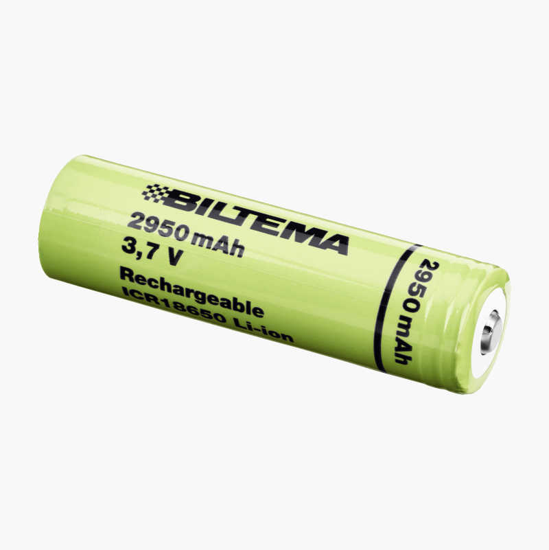
Too high termination voltage, or too high charging current can cause growth of lithium dendrites, that short + and -. Will end in flames. Always check manufacturer datasheet for charging curves and voltages
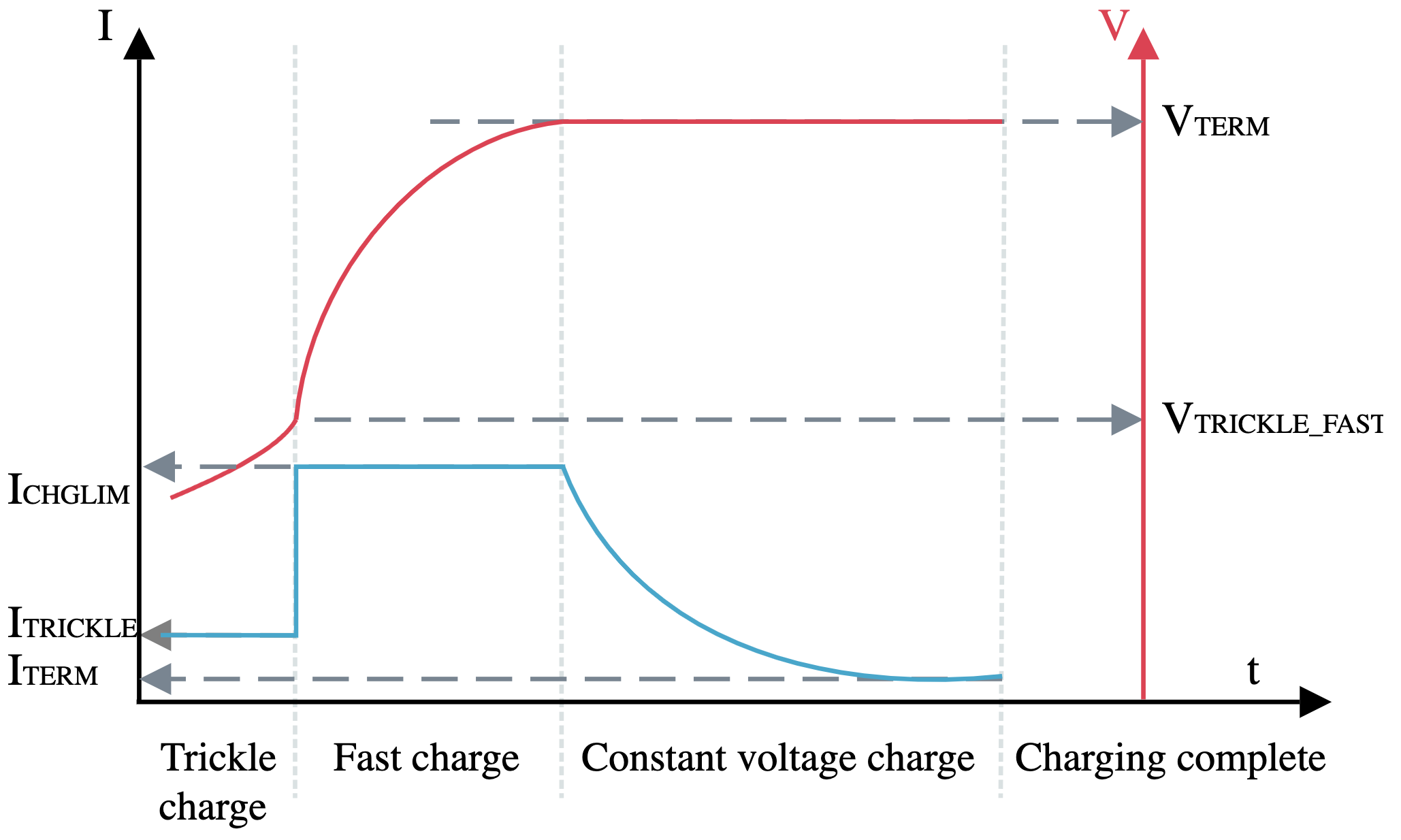
Battery charger - Inputs
Voltage above \(V_{TRICKLE}\)
Voltage close to \(V_{TERM}\)
If voltage close to \(V_{TERM}\) and current is close to \(I_{TERM}\), then charging complete
If charging complete, and voltage has dropped (\(V_{RECHARGE}\)), then start again
Battery charger - States
Trickle charge (0.1 C)
Fast charge (1 C)
Constant voltage
Charging complete

One way to draw FSMs - Graphviz
digraph finite_state_machine {
    rankdir=LR;
    size="8,5"

    node [shape = doublecircle, label="Trickle charger", fontsize=12] trkl;
    node [shape = circle, label="Fast charge", fontsize=12] fast;
    node [shape = circle, label="Const. Voltage", fontsize=12] vconst;
    node [shape = circle, label="Done", fontsize=12] done;

    trkl -> trkl [label="vtrkl = 0"];
    trkl -> fast [label="vtrkl = 1"];
    fast -> fast [label="vterm = 0"];
    fast -> vconst [label="vterm = 1"];
    vconst-> vconst [label="iterm = 0"];
    vconst-> done [label="iterm = 1"];
    done-> done [label="vrchrg = 0"];
    done-> trkl [label="vrchrg = 1"];

}
dot -Tpdf bcharger.dot -o bcharger.pdf
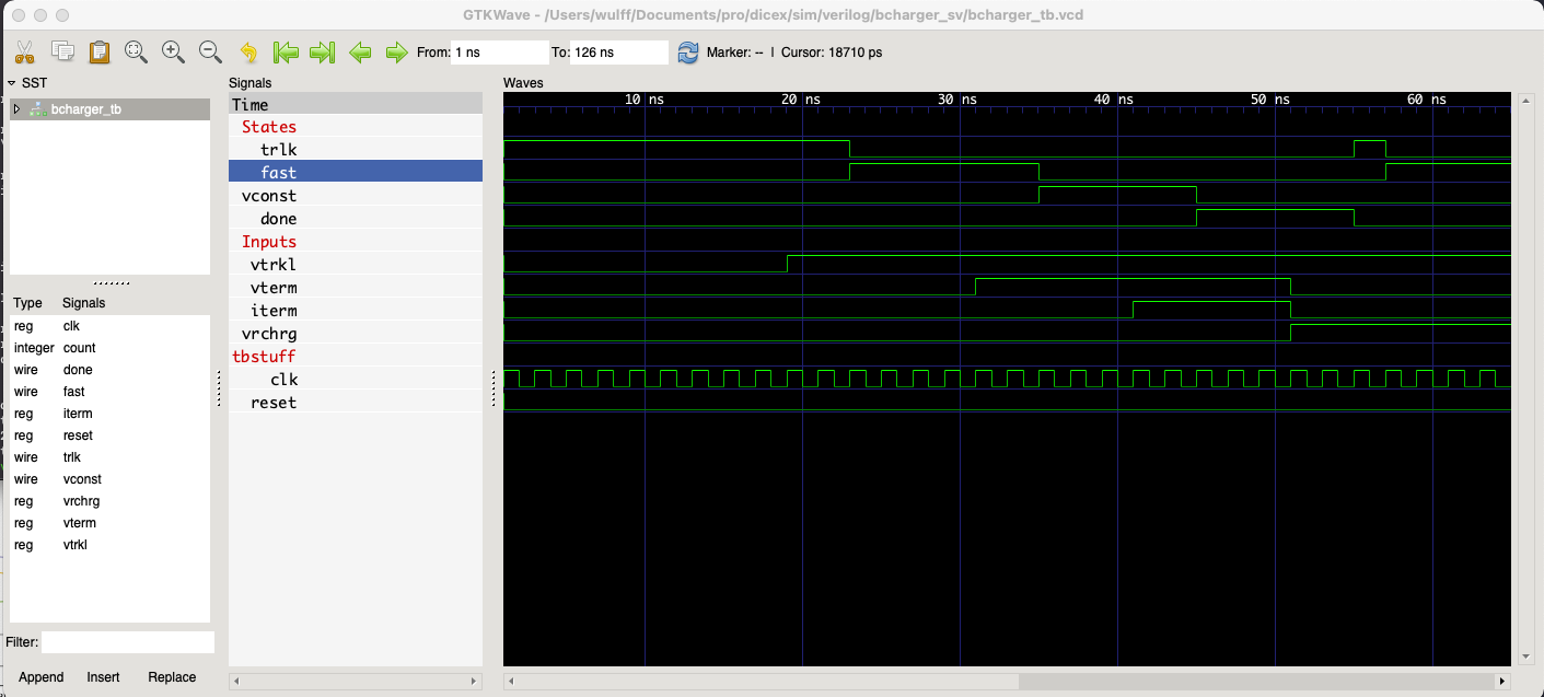
module bcharger( output logic trkl,
        output logic fast,
        output logic vconst,
        output logic done,
        input logic  vtrkl,
        input logic  vterm,
        input logic  iterm,
        input logic  vrchrg,
        input logic  clk,
        input logic  reset
                    );

   parameter TRLK = 0, FAST = 1, VCONST = 2, DONE=3;
   logic [1:0]                   state;
   logic [1:0]                   next_state;

   //- Figure out the next state
   always_comb begin
      case (state)
        TRLK: next_state = vtrkl ? FAST : TRLK;
        FAST: next_state = vterm ? VCONST : FAST;
        VCONST: next_state = iterm ? DONE : VCONST;
        DONE: next_state = vrchrg ? TRLK :DONE;
        default: next_state = TRLK;
      endcase // case (state)
    end
   //- Control output signals
   always_ff @(posedge clk or posedge reset) begin
      if(reset) begin
         state <= TRLK;
         trkl <= 1;
         fast <= 0;
         vconst <= 0;
         done <= 0;
      end
      else begin
         state <= next_state;
         case (state)
           TRLK: begin
              trkl <= 1;
              fast <= 0;
              vconst <= 0;
              done <= 0;
           end
           FAST: begin
              trkl <= 0;
              fast <= 1;
              vconst <= 0;
              done <= 0;

           end
           VCONST: begin
              trkl <= 0;
              fast <= 0;
              vconst <= 1;
              done <= 0;

           end
           DONE: begin
              trkl <= 0;
              fast <= 0;
              vconst <= 0;
              done <= 1;
           end
         endcase // case (state)
      end // else: !if(reset)
   end
endmodule
Synthesize FSM with yosys
dicex/sim/verilog/bcharger_sv/bcharger.ys
# read design
read_verilog -sv bcharger.sv;
hierarchy -top bcharger;

# the high-level stuff
fsm; opt; memory; opt;

# mapping to internal cell library
techmap; opt;
synth;
opt_clean;

# mapping flip-flops
dfflibmap  -liberty ../../../lib/SUN_TR_GF130N.lib

# mapping logic
abc -liberty ../../../lib/SUN_TR_GF130N.lib

# write synth netlist
write_verilog bcharger_netlist.v
read_verilog  ../../../lib/SUN_TR_GF130N_empty.v
write_spice -big_endian -neg AVSS -pos AVDD -top bcharger bcharger_netlist.sp

# write dot so we can make image
show -format dot -prefix bcharger_synth -colors 1 -width -stretch
clean
