cictikz
AI-driven TikZ circuit schematics
Symbol library
All coordinates are figure units (\grid = 1.6, one transistor
tall, y up) relative to the macro entry point. Macros are path
fragments: they start at the current point and compose inside one
\draw. Every rendering below is produced by the macro itself,
so this page doubles as a compile test of the library.
| symbol | description |
|---|---|
\anaQuestion |
Current mirror bias question figure (M1-M3 with sources) |
\cicAdd |
Summing node: circle with + |
\cicAnd |
AND gate, hand-rolled house shape |
\cicBuf |
Buffer (triangle, no bubble), hand-rolled house shape |
\cicBufM |
Buffer pointing left (for feedback paths); in right, out left |
\cicDff |
D flip-flop box: D and clock wedge left, Q and QN right; entry/exit lower-left |
\cicH |
Transfer-function box H(s) |
\cicInv |
Inverter, hand-rolled house shape; exports |
\cicInvM |
Inverter pointing left (for feedback paths); in right, out left |
\cicNand |
NAND gate, hand-rolled house shape; exports |
\cicNor |
NOR gate, hand-rolled house shape |
\cicOr |
OR gate, hand-rolled house shape |
\cicOta |
Fully differential OTA outline (triangle, +/- in, -/+ out). Exports coordinates cicOta_inp/inn/outp/outn; path returns to inp. |
\cicOtaSSWP |
Single-ended OTA outline with caller-set input labels |
\cicOtaSWP |
Fully differential OTA outline with caller-set port labels (+in/-in/+out/-out) |
\cicTgate |
Transmission gate: facing triangles, enable below, enable-bar bubble above |
\cmCascode |
Cascoded NMOS current mirror (M1-M4, v_b bias port), grounds included. Branches at x=0 and x=2.5, tops at y=3.7. Path returns to entry. |
\cmRCascode |
Cascode mirror with resistor-derived cascode bias |
\cmSfCascode |
Cascode current mirror biased as source follower (M3/M4 under M1/M2) |
\cmSourceDeg |
Source-degenerated current mirror (R_s under M1/M2), grounds included |
\cmStd |
Standard NMOS current mirror (M1 diode-connected, M2 output), grounds included, current arrows i_i/i_o. Path returns to entry. |
\curDown |
Downward current arrow on a half-grid stub |
\esdGgnmos |
Grounded-gate NMOS ESD clamp with gate resistor |
\filtActLP |
Active RC low-pass: R into OTA virtual ground, C in feedback |
\filtActZ |
Active filter with generic input/feedback impedances |
\filtHP |
Passive RC high-pass: series C to shunt R |
\filtLP |
Passive RC low-pass: series R to shunt C |
\hcapacitor |
Capacitor, horizontal |
\himpedance |
Generic impedance box, horizontal |
\hresistor |
Resistor, horizontal (hand-rolled zig-zag) |
\lvmnmos |
NMOS transistor, vertical, drain up, gate on the right (mirrored), with optional gate input port; gate pin is the end of the gate lead |
\lvmpmos |
PMOS transistor, vertical, source up, gate on the right (mirrored), with optional gate input port; gate pin is the end of the gate lead |
\lvnmos |
NMOS transistor, vertical, drain up, gate on the left, with optional gate input port; gate pin is the end of the gate lead |
\lvpmos |
PMOS transistor, vertical, source up, gate on the left, with optional gate input port; gate pin is the end of the gate lead |
\portCurDown |
Downward current arrow with a label |
\portDiffIn |
Differential input port pair (+ over -, 1.6 apart) |
\portDiffOut |
Differential output port pair (+ over -, 1.6 apart) |
\portIn |
Input port: open circle at the current point, label to the left (anchor east) |
\portOut |
Output port: junction dot at entry, 0.5 wire right, open circle, label right |
\portOutDown |
Output port drawn downward half a grid |
\portmIn |
Input port, mirrored: label to the right (anchor west), for mirrored devices |
\trNmos |
NMOS with labelled Gate/Drain/Source terminals (teaching figure) |
\vcapacitor |
Capacitor, vertical |
\vdiode |
Diode, vertical, anode down cathode up (compact house size) |
\vground |
Ground symbol (three shrinking bars, downward). Path returns to entry. |
\vimpedance |
Generic impedance box, vertical |
\vmnmos |
NMOS transistor, vertical, drain up, gate on the right (mirrored); gate pin is the end of the gate lead |
\vmpmos |
PMOS transistor, vertical, source up, gate on the right (mirrored); gate pin is the end of the gate lead |
\vnmos |
NMOS transistor, vertical, drain up, gate on the left; gate pin is the end of the gate lead |
\vpmos |
PMOS transistor, vertical, source up, gate on the left; gate pin is the end of the gate lead |
\vresistor |
Resistor, vertical (hand-rolled zig-zag, weight-matched to wires) |
\vsupply |
Supply symbol (upward stub with slash). Path returns to entry. |
\vvsource |
Voltage source, vertical, drawn DOWNWARD 1.5 grid from entry |
Transistors
esdGgnmos
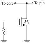
Grounded-gate NMOS ESD clamp with gate resistor
\esdGgnmos
entry [0, 0] — exit [0, 0]
| pin | position | direction |
|---|---|---|
| pin | [0.5, 3.2] | inout |
| core | [-1, 3.2] | inout |
exported coordinates: esdStart, cStart, esdRbot, top
\draw (0,0) \esdGgnmos;
lvmnmos

NMOS transistor, vertical, drain up, gate on the right (mirrored), with optional gate input port; gate pin is the end of the gate lead
\lvmnmos{instance name (becomes circuitikz node, e.g. M1)}{gate port label, e.g. $v_i$ (empty {} suppresses the port)}
entry [0, 0] — exit [0, 1.6]
| pin | position | direction |
|---|---|---|
| drain | [0, 1.6] | inout |
| gate | [0.98, 0.8] | in |
| source | [0, 0] | inout |
anchors: <inst>.drain, <inst>.gate, <inst>.source, <inst>.bulk
exported coordinates: cicmos
xschem: sky130_fd_pr/nfet_01v8.sym
\draw (0,0) \vground \lvmnmos{M1}{$v_i$};
lvmpmos

PMOS transistor, vertical, source up, gate on the right (mirrored), with optional gate input port; gate pin is the end of the gate lead
\lvmpmos{instance name (becomes circuitikz node, e.g. M1)}{gate port label, e.g. $v_i$ (empty {} suppresses the port)}
entry [0, 0] — exit [0, 1.6]
| pin | position | direction |
|---|---|---|
| source | [0, 1.6] | inout |
| gate | [0.98, 0.8] | in |
| drain | [0, 0] | inout |
anchors: <inst>.drain, <inst>.gate, <inst>.source, <inst>.bulk
exported coordinates: cicmos
xschem: sky130_fd_pr/pfet_01v8.sym
\draw (0,0) \vground \lvmpmos{M1}{$v_i$};
lvnmos

NMOS transistor, vertical, drain up, gate on the left, with optional gate input port; gate pin is the end of the gate lead
\lvnmos{instance name (becomes circuitikz node, e.g. M1)}{gate port label, e.g. $v_i$ (empty {} suppresses the port)}
entry [0, 0] — exit [0, 1.6]
| pin | position | direction |
|---|---|---|
| drain | [0, 1.6] | inout |
| gate | [-0.98, 0.8] | in |
| source | [0, 0] | inout |
anchors: <inst>.drain, <inst>.gate, <inst>.source, <inst>.bulk
exported coordinates: cicmos
xschem: sky130_fd_pr/nfet_01v8.sym
\draw (0,0) \vground \lvnmos{M1}{$v_i$};
lvpmos

PMOS transistor, vertical, source up, gate on the left, with optional gate input port; gate pin is the end of the gate lead
\lvpmos{instance name (becomes circuitikz node, e.g. M1)}{gate port label, e.g. $v_i$ (empty {} suppresses the port)}
entry [0, 0] — exit [0, 1.6]
| pin | position | direction |
|---|---|---|
| source | [0, 1.6] | inout |
| gate | [-0.98, 0.8] | in |
| drain | [0, 0] | inout |
anchors: <inst>.drain, <inst>.gate, <inst>.source, <inst>.bulk
exported coordinates: cicmos
xschem: sky130_fd_pr/pfet_01v8.sym
\draw (0,0) \vground \lvpmos{M1}{$v_i$};
trNmos

NMOS with labelled Gate/Drain/Source terminals (teaching figure)
\trNmos
entry [0, 0] — exit [0, 0]
| pin | position | direction |
|---|---|---|
| drain | [0, 1.6] | inout |
| gate | [-0.98, 0.8] | in |
| source | [0, 0] | inout |
exported coordinates: cStart
\draw (0,0) \trNmos;
vmnmos

NMOS transistor, vertical, drain up, gate on the right (mirrored); gate pin is the end of the gate lead
\vmnmos{instance name (becomes circuitikz node, e.g. M1)}
entry [0, 0] — exit [0, 1.6]
| pin | position | direction |
|---|---|---|
| drain | [0, 1.6] | inout |
| gate | [0.98, 0.8] | in |
| source | [0, 0] | inout |
anchors: <inst>.drain, <inst>.gate, <inst>.source, <inst>.bulk
xschem: sky130_fd_pr/nfet_01v8.sym
\draw (0,0) \vground \vmnmos{M1};
vmpmos

PMOS transistor, vertical, source up, gate on the right (mirrored); gate pin is the end of the gate lead
\vmpmos{instance name (becomes circuitikz node, e.g. M1)}
entry [0, 0] — exit [0, 1.6]
| pin | position | direction |
|---|---|---|
| source | [0, 1.6] | inout |
| gate | [0.98, 0.8] | in |
| drain | [0, 0] | inout |
anchors: <inst>.drain, <inst>.gate, <inst>.source, <inst>.bulk
xschem: sky130_fd_pr/pfet_01v8.sym
\draw (0,0) \vground \vmpmos{M1};
vnmos

NMOS transistor, vertical, drain up, gate on the left; gate pin is the end of the gate lead
\vnmos{instance name (becomes circuitikz node, e.g. M1)}
entry [0, 0] — exit [0, 1.6]
| pin | position | direction |
|---|---|---|
| drain | [0, 1.6] | inout |
| gate | [-0.98, 0.8] | in |
| source | [0, 0] | inout |
anchors: <inst>.drain, <inst>.gate, <inst>.source, <inst>.bulk
xschem: sky130_fd_pr/nfet_01v8.sym
\draw (0,0) \vground \vnmos{M1};
vpmos

PMOS transistor, vertical, source up, gate on the left; gate pin is the end of the gate lead
\vpmos{instance name (becomes circuitikz node, e.g. M1)}
entry [0, 0] — exit [0, 1.6]
| pin | position | direction |
|---|---|---|
| source | [0, 1.6] | inout |
| gate | [-0.98, 0.8] | in |
| drain | [0, 0] | inout |
anchors: <inst>.drain, <inst>.gate, <inst>.source, <inst>.bulk
xschem: sky130_fd_pr/pfet_01v8.sym
\draw (0,0) \vground \vpmos{M1};
Passives
hcapacitor

Capacitor, horizontal
\hcapacitor{value label, e.g. $R_s$}
entry [0, 0] — exit [1.6, 0]
| pin | position | direction |
|---|---|---|
| minus | [0, 0] | inout |
| plus | [1.6, 0] | inout |
exported coordinates: cStart, capEnd
xschem: devices/capa.sym
\draw (0,0) \hcapacitor{$Z$};
himpedance

Generic impedance box, horizontal
\himpedance{value label, e.g. $R_s$}
entry [0, 0] — exit [1.6, 0]
| pin | position | direction |
|---|---|---|
| minus | [0, 0] | inout |
| plus | [1.6, 0] | inout |
exported coordinates: cStart, impEnd
\draw (0,0) \himpedance{$Z$};
hresistor

Resistor, horizontal (hand-rolled zig-zag)
\hresistor{value label, e.g. $R_s$}
entry [0, 0] — exit [1.6, 0]
| pin | position | direction |
|---|---|---|
| minus | [0, 0] | inout |
| plus | [1.6, 0] | inout |
exported coordinates: cStart, resEnd
xschem: devices/res.sym
\draw (0,0) \hresistor{$Z$};
vcapacitor

Capacitor, vertical
\vcapacitor{value label, e.g. $R_s$}
entry [0, 0] — exit [0, 1.6]
| pin | position | direction |
|---|---|---|
| minus | [0, 0] | inout |
| plus | [0, 1.6] | inout |
exported coordinates: cStart, capEnd
xschem: devices/capa.sym
\draw (0,0) \vcapacitor{$Z$};
vimpedance

Generic impedance box, vertical
\vimpedance{value label, e.g. $R_s$}
entry [0, 0] — exit [0, 1.6]
| pin | position | direction |
|---|---|---|
| minus | [0, 0] | inout |
| plus | [0, 1.6] | inout |
exported coordinates: cStart, impEnd
\draw (0,0) \vimpedance{$Z$};
vresistor

Resistor, vertical (hand-rolled zig-zag, weight-matched to wires)
\vresistor{value label, e.g. $R_s$}
entry [0, 0] — exit [0, 1.6]
| pin | position | direction |
|---|---|---|
| minus | [0, 0] | inout |
| plus | [0, 1.6] | inout |
exported coordinates: cStart, resEnd
xschem: devices/res.sym
\draw (0,0) \vresistor{$Z$};
Sources and rails
vground

Ground symbol (three shrinking bars, downward). Path returns to entry.
\vground
entry [0, 0] — exit [0, 0]
| pin | position | direction |
|---|---|---|
| term | [0, 0] | supply |
exported coordinates: cStart
xschem: devices/gnd.sym
\draw (0,0) \vground \vresistor{$R$};
vsupply

Supply symbol (upward stub with slash). Path returns to entry.
\vsupply
entry [0, 0] — exit [0, 0]
| pin | position | direction |
|---|---|---|
| term | [0, 0] | supply |
exported coordinates: vSupplyStart
xschem: devices/vdd.sym
\draw (M3.drain) \vsupply;
vvsource

Voltage source, vertical, drawn DOWNWARD 1.5 grid from entry
\vvsource{source label, e.g. $V_{DD}$}
entry [0, 0] — exit [0, -2.4]
| pin | position | direction |
|---|---|---|
| plus | [0, 0] | inout |
| minus | [0, -2.4] | inout |
xschem: devices/vsource.sym
\draw (0,0) \vvsource{$V_{DD}$} \vground;
Ports
curDown

Downward current arrow on a half-grid stub
\curDown{current label}
entry [0, 0] — exit [0, -0.8]
| pin | position | direction |
|---|---|---|
| term | [0, 0] | inout |
\draw (0,0) \curDown{x};
portCurDown

Downward current arrow with a label
\portCurDown{current label}
entry [0, 0] — exit [0, -0.8]
| pin | position | direction |
|---|---|---|
| term | [0, 0] | inout |
\draw (0,0) \portCurDown{x};
portDiffIn

Differential input port pair (+ over -, 1.6 apart)
\portDiffIn{port label}
entry [0, 0] — exit [0, 0]
| pin | position | direction |
|---|---|---|
| plus | [0, 0] | in |
| minus | [0, -1.6] | in |
exported coordinates: cStart
\draw (0,0) \portDiffIn{x};
portDiffOut

Differential output port pair (+ over -, 1.6 apart)
\portDiffOut{port label}
entry [0, 0] — exit [0, 0]
| pin | position | direction |
|---|---|---|
| plus | [0.5, 0] | out |
| minus | [0.5, -1.6] | out |
exported coordinates: cStart
\draw (0,0) \portDiffOut{x};
portIn

Input port: open circle at the current point, label to the left (anchor east)
\portIn{port label, e.g. $v_i$}
entry [0, 0] — exit [0, 0]
| pin | position | direction |
|---|---|---|
| term | [0, 0] | in |
xschem: devices/ipin.sym
\draw (M1.gate) \portIn{$v_i$};
portOut

Output port: junction dot at entry, 0.5 wire right, open circle, label right
\portOut{port label, e.g. $v_o$}
entry [0, 0] — exit [0.5, 0]
| pin | position | direction |
|---|---|---|
| term | [0, 0] | out |
xschem: devices/opin.sym
\draw (M1.drain) \portOut{$v_o$};
portOutDown

Output port drawn downward half a grid
\portOutDown{port label}
entry [0, 0] — exit [0, -0.8]
| pin | position | direction |
|---|---|---|
| term | [0, 0] | out |
exported coordinates: cStart
\draw (0,0) \portOutDown{x};
portmIn

Input port, mirrored: label to the right (anchor west), for mirrored devices
\portmIn{port label}
entry [0, 0] — exit [0, 0]
| pin | position | direction |
|---|---|---|
| term | [0, 0] | in |
xschem: devices/ipin.sym
\draw (M2.gate) \portmIn{$v_b$};
OTAs and blocks
cicAdd

Summing node: circle with +
\cicAdd
entry [0, 0] — exit [0.4, 0]
| pin | position | direction |
|---|---|---|
| in | [0, 0] | in |
| out | [0.4, 0] | out |
\draw (0,0) \cicAdd;
cicAnd

AND gate, hand-rolled house shape
\cicAnd{instance name}
entry [0, 0] — exit [1.18, 0]
| pin | position | direction |
|---|---|---|
| in1 | [0, 0.32] | in |
| in2 | [0, -0.32] | in |
| out | [1.18, 0] | out |
\draw (0,0) \cicAnd{x};
cicBuf

Buffer (triangle, no bubble), hand-rolled house shape
\cicBuf{instance name}
entry [0, 0] — exit [0.9, 0]
| pin | position | direction |
|---|---|---|
| in | [0, 0] | in |
| out | [0.9, 0] | out |
\draw (0,0) \cicBuf{x};
cicBufM

Buffer pointing left (for feedback paths); in right, out left
\cicBufM{instance name}
entry [0, 0] — exit [-0.9, 0]
| pin | position | direction |
|---|---|---|
| in | [0, 0] | in |
| out | [-0.9, 0] | out |
\draw (0,0) \cicBufM{x};
cicDff

D flip-flop box: D and clock wedge left, Q and QN right; entry/exit lower-left
\cicDff{instance name}
entry [0, 0] — exit [0, 0]
| pin | position | direction |
|---|---|---|
| d | [0, 1.5] | in |
| ck | [0, 0.4] | in |
| q | [1.6, 0.4] | out |
| qn | [1.6, 1.5] | out |
\draw (0,0) \cicDff{x};
cicH

Transfer-function box H(s)
\cicH{box label}
entry [0, 0] — exit [0.8, 0]
| pin | position | direction |
|---|---|---|
| in | [0, 0] | in |
| out | [0.8, 0] | out |
\draw (0,0) \cicH{x};
cicInv

Inverter, hand-rolled house shape; exports
\cicInv{instance name}
entry [0, 0] — exit [1.1, 0]
| pin | position | direction |
|---|---|---|
| in | [0, 0] | in |
| out | [1.1, 0] | out |
\draw (0,0) \cicInv{x};
cicInvM

Inverter pointing left (for feedback paths); in right, out left
\cicInvM{instance name}
entry [0, 0] — exit [-1.1, 0]
| pin | position | direction |
|---|---|---|
| in | [0, 0] | in |
| out | [-1.1, 0] | out |
\draw (0,0) \cicInvM{x};
cicNand

NAND gate, hand-rolled house shape; exports
\cicNand{instance name, e.g. g1}
entry [0, 0] — exit [1.38, 0]
| pin | position | direction |
|---|---|---|
| in1 | [0, 0.32] | in |
| in2 | [0, -0.32] | in |
| out | [1.38, 0] | out |
\draw (0,0) \cicNand{g1};
\draw (-0.5,0.32) -- (g1_in1);
cicNor

NOR gate, hand-rolled house shape
\cicNor{instance name}
entry [0, 0] — exit [1.7, 0]
| pin | position | direction |
|---|---|---|
| in1 | [0, 0.32] | in |
| in2 | [0, -0.32] | in |
| out | [1.7, 0] | out |
\draw (0,0) \cicNor{x};
cicOr

OR gate, hand-rolled house shape
\cicOr{instance name}
entry [0, 0] — exit [1.5, 0]
| pin | position | direction |
|---|---|---|
| in1 | [0, 0.32] | in |
| in2 | [0, -0.32] | in |
| out | [1.5, 0] | out |
\draw (0,0) \cicOr{x};
cicOta

Fully differential OTA outline (triangle, +/- in, -/+ out). Exports coordinates cicOta_inp/inn/outp/outn; path returns to inp.
\cicOta
entry [0, 0] — exit [0, 0]
| pin | position | direction |
|---|---|---|
| inp | [0, 0] | in |
| inn | [0, -1.6] | in |
| outp | [2.6, -1.6] | out |
| outn | [2.6, 0] | out |
anchors: cicOta_inp, cicOta_inn, cicOta_outp, cicOta_outn
exported coordinates: cicOta_inp, cicOta_inn, cicOta_outp, cicOta_outn
\draw (0,0) \cicOta;
\draw (cicOta_inp) \portIn{$v_{ip}$};
\draw (cicOta_outn) \portOut{$v_{on}$};
cicOtaSSWP

Single-ended OTA outline with caller-set input labels
\cicOtaSSWP{+in label}{-in label}
entry [0, 0] — exit [0, 0]
| pin | position | direction |
|---|---|---|
| inp | [0, 0] | in |
| inn | [0, -0.8] | in |
| out | [2.6, -0.4] | out |
exported coordinates: cicOtaS_inp, cicOtaS_inn, cicOtaS_out
\draw (0,0) \cicOtaSSWP{x}{x};
cicOtaSWP

Fully differential OTA outline with caller-set port labels (+in/-in/+out/-out)
\cicOtaSWP{+in label}{-in label}{+out label}{-out label}
entry [0, 0] — exit [0, 0]
| pin | position | direction |
|---|---|---|
| inp | [0, 0] | in |
| inn | [0, -1.6] | in |
| outp | [2.6, -1.6] | out |
| outn | [2.6, 0] | out |
exported coordinates: cicOta_inp, cicOta_inn, cicOta_outp, cicOta_outn
\draw (0,0) \cicOtaSWP{x}{x}{x}{x};
cicTgate

Transmission gate: facing triangles, enable below, enable-bar bubble above
\cicTgate{instance name}
entry [0, 0] — exit [1.4, 0]
| pin | position | direction |
|---|---|---|
| in | [0, 0] | in |
| out | [1.4, 0] | out |
| en | [0.7, -0.55] | in |
| enb | [0.7, 0.64] | in |
\draw (0,0) \cicTgate{x};
Current mirrors
cmCascode
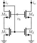
Cascoded NMOS current mirror (M1-M4, v_b bias port), grounds included. Branches at x=0 and x=2.5, tops at y=3.7. Path returns to entry.
\cmCascode
entry [0, 0] — exit [0, 0]
| pin | position | direction |
|---|---|---|
| in | [0, 3.7] | in |
| out | [2.5, 3.7] | out |
anchors: mn1.gate, mn2.gate, mn3.gate, mn4.gate, mn3.drain
exported coordinates: cStart
\draw (0,0) \cmCascode;
cmRCascode
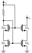
Cascode mirror with resistor-derived cascode bias
\cmRCascode
entry [0, 0] — exit [0, 0]
| pin | position | direction |
|---|---|---|
| in | [0, 5.3] | in |
| out | [2.5, 3.7] | out |
exported coordinates: cmRStart, cStart, resCon, resEnd
\draw (0,0) \cmRCascode;
cmSfCascode
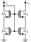
Cascode current mirror biased as source follower (M3/M4 under M1/M2)
\cmSfCascode
entry [0, 0] — exit [0, 0]
| pin | position | direction |
|---|---|---|
| in | [0, 3.7] | in |
| out | [2, 3.7] | out |
exported coordinates: cStart
\draw (0,0) \cmSfCascode;
cmSourceDeg
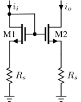
Source-degenerated current mirror (R_s under M1/M2), grounds included
\cmSourceDeg
entry [0, 0] — exit [0, 0]
| pin | position | direction |
|---|---|---|
| in | [0, 3.7] | in |
| out | [2, 3.7] | out |
exported coordinates: cStart
\draw (0,0) \cmSourceDeg;
cmStd
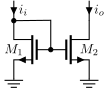
Standard NMOS current mirror (M1 diode-connected, M2 output), grounds included, current arrows i_i/i_o. Path returns to entry.
\cmStd
entry [0, 0] — exit [0, 0]
| pin | position | direction |
|---|---|---|
| in | [0, 2.1] | in |
| out | [2.0, 2.1] | out |
anchors: mn1.gate, mn1.drain, mn2.gate, mn2.drain
exported coordinates: cStart
\draw (0,0) \cmStd;
Filters
filtActLP
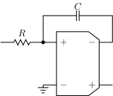
Active RC low-pass: R into OTA virtual ground, C in feedback
\filtActLP{R label}{C label}
entry [0, 0] — exit [4.2, 0]
| pin | position | direction |
|---|---|---|
| in | [0, 0] | in |
| out | [4.2, 0] | out |
exported coordinates: cicStart, resEnd, capEnd, cStart, cicOta_inp, cicOta_inn, cicOta_outp, cicOta_outn
\draw (0,0) \filtActLP{x}{x};
filtActZ
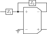
Active filter with generic input/feedback impedances
\filtActZ{input Z label}{feedback Z label}
entry [0, 0] — exit [4.2, 0]
| pin | position | direction |
|---|---|---|
| in | [0, 0] | in |
| out | [4.2, 0] | out |
exported coordinates: cicStart, impEnd, cStart, cicOta_inp, cicOta_inn, cicOta_outp, cicOta_outn
\draw (0,0) \filtActZ{x}{x};
filtHP

Passive RC high-pass: series C to shunt R
\filtHP{C label}{R label}
entry [0, 0] — exit [1.6, 0]
| pin | position | direction |
|---|---|---|
| in | [0, 0] | in |
| out | [1.6, 0] | out |
exported coordinates: cStart, capEnd, resEnd
\draw (0,0) \filtHP{x}{x};
filtLP

Passive RC low-pass: series R to shunt C
\filtLP{R label}{C label}
entry [0, 0] — exit [1.6, 0]
| pin | position | direction |
|---|---|---|
| in | [0, 0] | in |
| out | [1.6, 0] | out |
exported coordinates: cStart, resEnd, capEnd
\draw (0,0) \filtLP{x}{x};
Other
anaQuestion
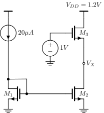
Current mirror bias question figure (M1-M3 with sources)
\anaQuestion
entry [0, 0] — exit [0, 0]
exported coordinates: cStart
\draw (0,0) \anaQuestion;
vdiode

Diode, vertical, anode down cathode up (compact house size)
\vdiode{label, e.g. $D_1$}
entry [0, 0] — exit [0, 1.6]
| pin | position | direction |
|---|---|---|
| anode | [0, 0] | inout |
| cathode | [0, 1.6] | inout |
exported coordinates: cStart, diodeEnd
\draw (0,0) \vground \vdiode{$D_1$};