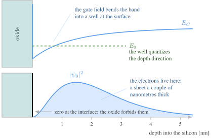
Metal Oxide Semiconductor
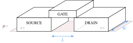
2
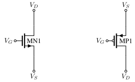
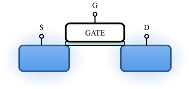
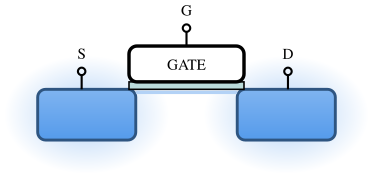
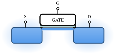
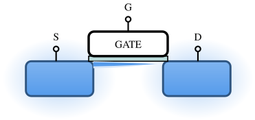
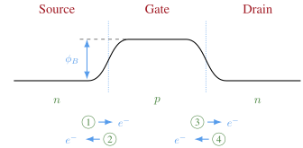
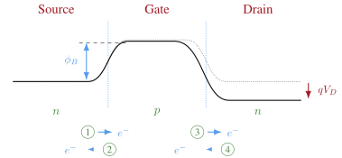
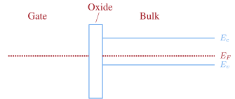
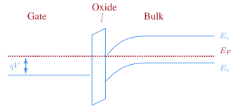
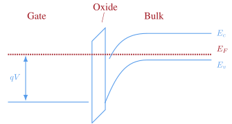
\[I_{DS} = f(V_{GS},V_{DS},...)\]
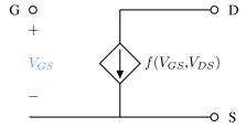
| Param | Voltage |
|---|---|
| VGS | 0 to 1.8 |
| VDS | 1.0 |
| VS | 0 |
| VB | 0 |
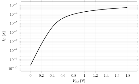
Define \(V_{eff} \equiv V_{GS} - V_{tn}\) , where \(V_{tn}\) is the "threshold voltage"
| Veff | Inversion level |
|---|---|
| less than 0 | weak inversion or subthreshold |
| 0 | moderate inversion |
| more than 100 mV | strong inversion |
Weak inversion
The drain current is low, but not zero, when
\[V_{eff} << 0\]
\[I_{DS} \approx I_{D0} \frac{W}{L} e^{V_{eff}/n V_{T}} \text{ if } V_{DS} > 3 V_{T}\]
\[n \approx 1.5\]
Moderate inversion
Very useful region in real designs. Hard for hand-calculation. Trust the model.
Strong inversion
\[I_{DS} = \mu_n C_{ox} \frac{W}{L} \begin{cases} V_{eff} V_{DS} & \text{if }V_{DS} << V_{eff} \\[15pt] V_{eff} V_{DS} - V_{DS}^2/2 & \text{if } V_{DS} < V_{eff} \\[15pt] \frac{1}{2} V_{eff}^2 & \text{if } V_{DS} > V_{eff} \\[15pt] \end{cases}\]
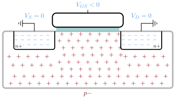
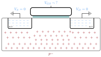
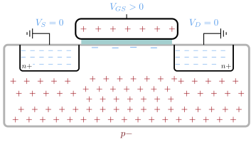
| Param | Voltage [V] |
|---|---|
| VGS | 0.5 |
| VDS | 0 to 1.8 |
| VS | 0 |
| VB | 0 |
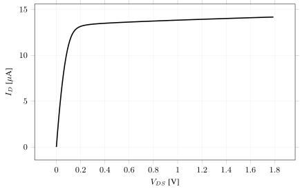
\[I_{DS} = \mu_n C_{ox} \frac{W}{L} \begin{cases} V_{eff} V_{DS} & \text{if }V_{DS} << V_{eff} \\[15pt] V_{eff} V_{DS} - V_{DS}^2/2 & \text{if } V_{DS} < V_{eff} \\[15pt] \frac{1}{2} V_{eff}^2 & \text{if } V_{DS} > V_{eff} \\[15pt] \end{cases}\]
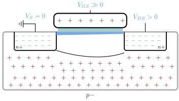
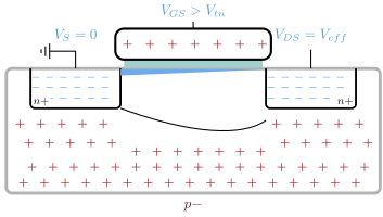
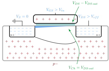
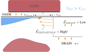
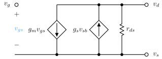
\[g_{m} = \frac{\partial I_{DS}}{\partial V_{GS}}\]
\[g_{ds} = \frac{1}{r_{ds}} = \frac{\partial I_{DS}}{\partial V_{DS}}\]
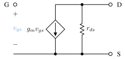
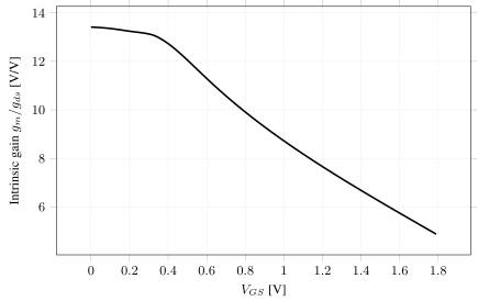
Define intrinsic gain as
\[A = \left\vert \frac{v_{out}}{v_{in}}\right\vert = g_m r_{ds} = \frac{g_m}{g_{ds}}\]
\[A = \frac{2 I_D}{V_{eff}} \times \frac{1}{ \lambda I_D } = \frac{2}{\lambda V_{eff}}\]
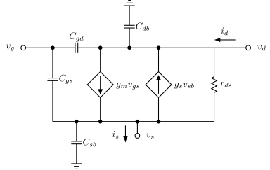
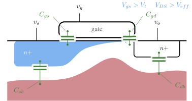
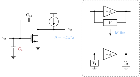
If \(Y(s) = 1/sC\) then \(Y_1(s) = 1/sC_{in}\) and \(Y_2(s) = 1/sC_{out}\) where \(C_{in} = (1 + A) C\), \(C_{out} = (1 + \frac{1}{A})C\)
\[C_{in} \approx C_{gd}\, g_{m} r_{ds}\]
\(C_{gd}\) can appear to be 10 to 100 times larger!
if gain from input to output is large
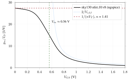
If \(V_{eff} < 0\) diffusion currents dominate.
\(I_{D} = I_{D0} \frac{W}{L} e^{V_{eff} / n V_T}\), where
\(V_T = kT/q\), \(n = (C_{ox} + C_{j0})/C_{ox}\)
\[I_{D0} = (n - 1) \mu_n C_{ox} V_T^2\]
\[g_m = \frac{I_D}{nV_T}\]
Bang for the buck
Subthreshold:
\(\frac{g_m}{I_D} = \frac{1}{nV_T} \approx 25.6 \text{ [S/A] @ 300 K}\)
Strong inversion:
\(\frac{g_m}{I_D} = \frac{2}{V_{eff}}\)
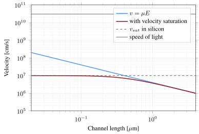
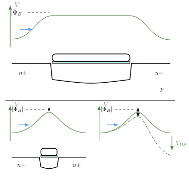
Electron speed limit in silicon
\[v \approx 10^7 cm/s\]
\[v = \mu_n E = \mu_n \frac{dV}{dx}\]
\(\mu_n \approx 100 \text{ to } 600 \text{ } cm^2/Vs\) in nanoscale CMOS
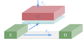
| Stress | PMOS | NMOS |
|---|---|---|
| Stretch Fz | Good | Good |
| Compress Fy | OK | Good |
| Compress Fx | Good | Bad |
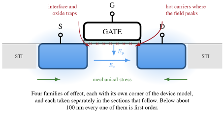
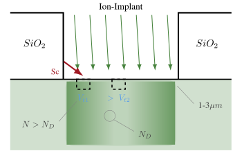
What can change stress?
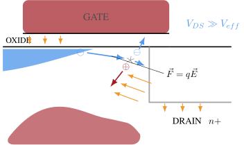
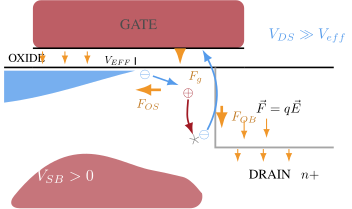
Provide \(I_2 = 1 \mu A\)
Let's use off-chip resistor \(R\), and pick \(R\) such that \(I_1 = 1 \mu A\)
Use \(\frac{W_1}{L_1} = \frac{W_2}{L_2}\)
What makes \(I_2 \ne 1 \mu A\)?
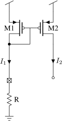
\[I_1 = \frac{V_{DD} - V_{GS1}}{R}\]
If \(V_{DD}\) changes, then current changes.
Fix: Keep \(V_{DD}\) constant
If \(V_{DS1} \ne V_{DS2} \rightarrow I_1 \ne I_2\)
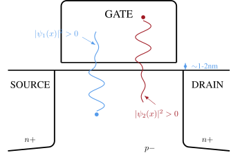
If layout direction of \(M_1 \ne M_2 \rightarrow I_1 \ne I_2\)
If current direction of \(M_1 \ne M_2 \rightarrow I_1 \ne I_2\)
If \(V_{S1} \ne V_{S2} \rightarrow I_1 \ne I_2\)
If \(V_{B1} \ne V_{B2} \rightarrow I_1 \ne I_2\)
If \(WPE_{1} \ne WPE_{2} \rightarrow I_1 \ne I_2\)
If \(Stress_{1} \ne Stress_{2} \rightarrow I_1 \ne I_2\) ...
Assume strong inversion and active \(V_{eff} = \sqrt{\frac{2}{\mu_p C_{ox} \frac{W}{L}} I_1}\), \(V_{GS} = V_{eff} + V_{tp}\)
\(I_1 = \frac{V_{DD} - V_{GS}}{R} = \frac{V_{DD} - \sqrt{\frac{2}{\mu_p C_{ox} \frac{W}{L}} I_1} - V_{tp}}{R}\)
\(\mu_p\), \(C_{ox}\), \(V_{tp}\) will all vary from die to die, and wafer lot to wafer lot.
Common to use 5 corners, or Monte-Carlo process simulation
| Corner | NMOS | PMOS |
|---|---|---|
| Mtt | Typical | Typical |
| Mss | Slow | Slow |
| Mff | Fast | Fast |
| Msf | Slowish | Fastish |
| Mfs | Fastish | Slowish |
Use calibration: measure error, tune circuit to fix error
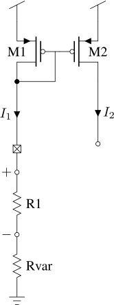
For every single chip, measure voltage across known resistor \(R_1\) and tune \(R_{var}\) such that we get \(I_1 = 1 \mu A\)
Be careful with multimeters, they have finite input resistance (typically 10 M\(\Omega\))
What is fast? High temperature or low temperature?
Fast corner - Mff (high mobility, low threshold voltage) - High \(V_{DD}\) - High or low temperature
Slow corner - Mss (low mobility, high threshold voltage) - Low \(V_{DD}\) - High or low temperature
Accept it, or don't use this circuit.
If you need stability over temperature, use 7.3.2 and 7.3.4 in CJM (SUN_BIAS_GF130N)
\(\frac{\sigma_{I_D}^2}{I_D^2} = \frac{1}{WL}\left[\left(\frac{gm}{I_D}\right)^2 \sigma_{vt}^2 + \frac{\sigma_{\ell}^2}{\ell^2}\right]\) \(\frac{\sigma_{I_D}}{I_D} \propto \frac{1}{\sqrt{WL}}\)
Assume \(\frac{\sigma_{I_D}}{I_D} = 10\%\), We want \(5\%\), how much do we need to change WL?
\[\frac{\frac{\sigma_{I_D}}{I_D}}{2} \propto \frac{1}{2\sqrt{WL}} = \frac{1}{\sqrt{4WL}}\]
We must quadruple the area to half the standard deviation
\(1 \%\) would require 100 times the area
\[\frac{\sigma_{I_D}^2}{I_D^2} = \frac{1}{WL}\left[\left(\frac{gm}{I_D}\right)^2 \sigma_{vt}^2 + \frac{\sigma_{\ell}^2}{\ell^2}\right]\]
Strong inversion \(\Rightarrow \frac{gm}{I_D} = \frac{2}{V_{eff}} = low\)
Weak inversion \(\Rightarrow \frac{gm}{I_D} = \frac{q}{n k T} \approx 25\)
Current mirrors achieve best matching in strong inversion
\[\frac{\sigma_{I_D}^2}{I_D^2} = \frac{1}{WL}\left[\left(\frac{gm}{I_D}\right)^2 \sigma_{vt}^2 + \frac{\sigma_{\ell}^2}{\ell^2}\right]\]
\[\sigma_{I_D}^2 = \frac{1}{WL}\left[gm^2 \sigma_{vt}^2 + I_D^2\frac{\sigma_{\ell}^2}{\ell^2}\right]\]
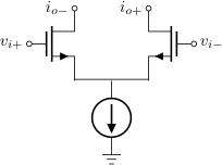
Offset voltage for a differential pair
\[i_o = i_{o+} - i_{o-} = g_m v_i = g_m (v_{i+} - v_{i-})\]
\[\sigma_{v_i}^2 = \frac{\sigma_{I_D}^2}{gm^2} = \frac{1}{WL}\left[\sigma_{vt}^2 + \frac{I_D^2}{gm^2}\frac{\sigma_{\ell}^2}{\ell^2}\right]\]
High \(\frac{gm}{I_D}\) is better (best in weak inversion)
Thermal noise Random scattering of carriers in the channel \(PSD_{TH}(f) = \text{Constant}\)
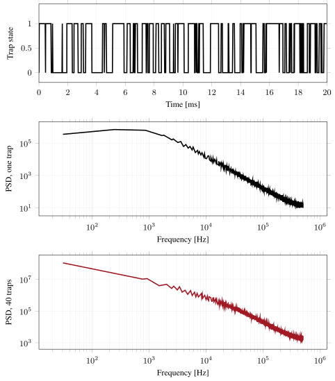
Popcorn noise Carriers get "stuck" in oxide traps (dangling bonds) for a while. Can cause a short-lived (seconds to minutes) shift in threshold voltage \(PSD_{GR}(f) \propto \text{Lorentzian shape} \approx \frac{A}{1 + \left(\frac{f}{f_0}\right)^2}\)
Flicker noise Assume there are many sources of popcorn noise at different energy levels and time constants, then the sum of the spectral densities approaches flicker noise. \(PSD_{flicker}(f) \propto \frac{1}{f}\)