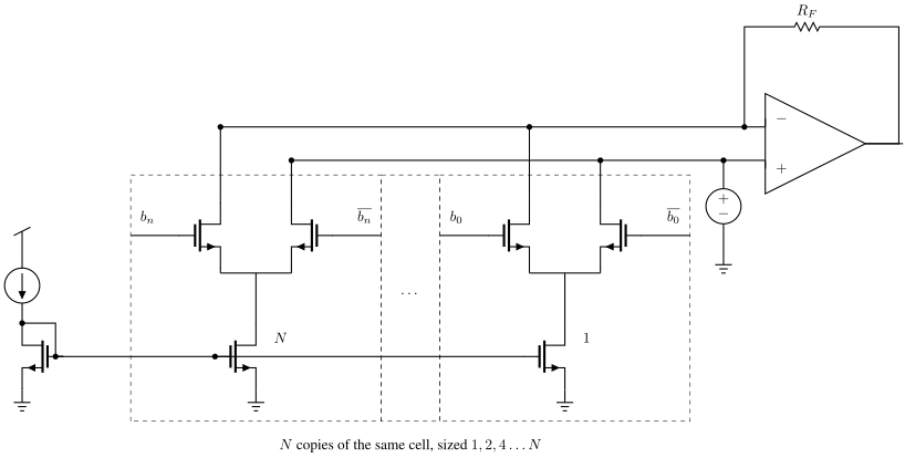
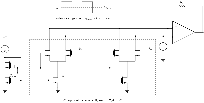
Digital to Analog Conversion

1

\[I_{out} = D_{in} \times I_{ref}\text{ [I]}\]

\[t_{out} = D_{in} \times t_{ref}\text{ [s]}\]

\[Q_{out} = D_{in} \times Q_{ref}\text{ [C]}\]

\[V_{out} = D_{in} \times V_{ref}\text{ [V]}\]

\[R_{out} = D_{in} \times R_{ref}\text{ [}\Omega\text{]}\]

The digital value is dimensionless, as such, there must be a reference value

2
Digital to analog conversion can be indirect through the relations between voltage, resistance, current, time, inductance and capacitance.

\[V = R I\]

\(Q = C V\)

\[dt = \frac{C dV}{I}\]

\[dt = \frac{L dI}{V}\]

3

Resistor based DACs

4

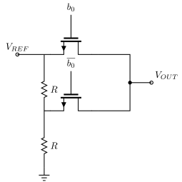
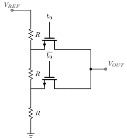
\[I_{ref} = \frac{V_{ref}}{3 R}\]

\[V_{out} = D_{in} R I_{ref} = \frac{D_{in} R V_{ref}}{3 R} \text{ [V]}\]

\[V_{out} = \frac{b_0 2 R V_{ref}}{3 R} + \frac{\overline{b_0} R V_{ref}}{3 R}\]

\[V_{out} = \begin{cases} \frac{2}{3} V_{ref}, & b_0 = 1 \\ \frac{1}{3} V_{ref}, & b_0 = 0 \end{cases}\]

5

\[I_{ref} = \frac{V_{ref}}{2 R}\]

\[V_{out} = \frac{b_0 2 R V_{ref}}{2 R} + \frac{\overline{b_0} R V_{ref}}{2 R}\]

\[V_{out} = \begin{cases} V_{ref}, & b_0 = 1 \\ \frac{1}{2} V_{ref}, & b_0 = 0 \end{cases}\]

6
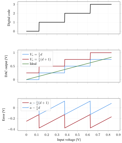
b Vo/Vr Vo/Vr
00 1/4 0/4
01 2/4 1/4
10 3/4 2/4
11 4/4 3/4

What is correct?

7

DAC errors

8

Digital to analog converters do not add quantization error. The quantization error is already in the digital word.

\[V_{out} = B + a_1 D_{in} + \left( a_2 D_{in}^2 + \dots + a_n D_{in}^n \right)\]

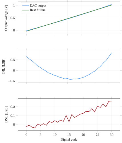
DAC output will contain gain errors, offset errors, and non-linear components

9

\[DNL[k] = \frac{V[k+1] - V[k]}{V_{LSB}} - 1\]

\[INL[k] = \frac{V[k] - V_{ideal}[k]}{V_{LSB}}\]

10

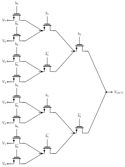
DAC complexity

11

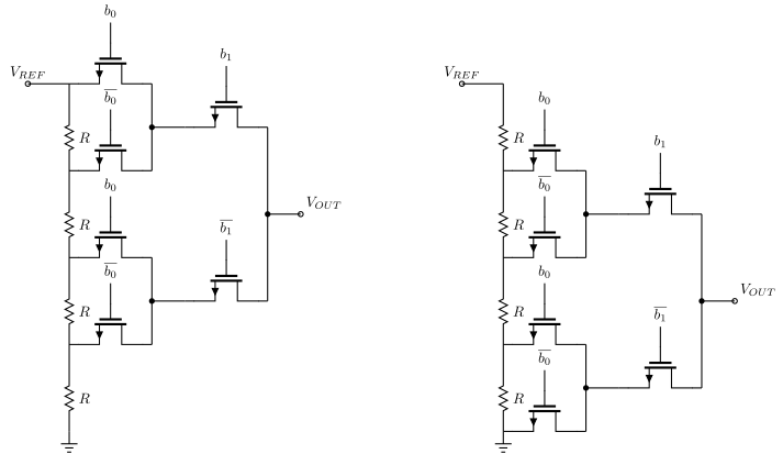
As number of resistors grow, the switches grow as

\[\sum_{n=1}^{N} 2^n = 2^{N+1} - 2\]

12

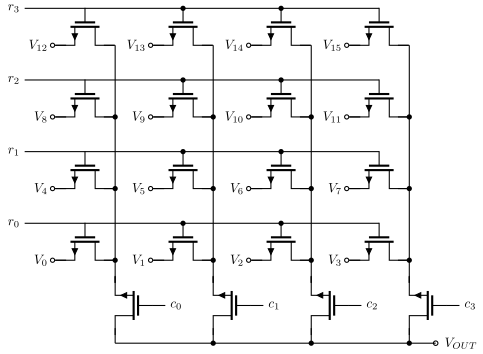
Give every tap a switch onto a column line, and every column line a switch to the output. For \(2^N\) taps in a square arrangement that is

\[2^{N} + 2^{N/2}\]

13

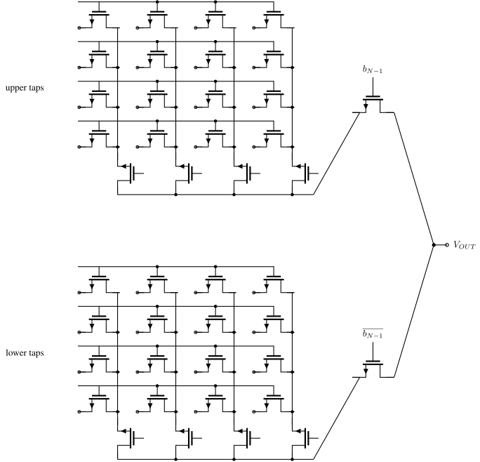
Switches in a 10-bit digital to analog converter.

\[\begin{array}{lll} \text{Tree} & 2^{N+1}-2 & = 2046 \\ \text{Matrix} & 2^{N} + 2^{N/2} & = 1056 \\ \text{Two strings, 6b + 4b} & 2^{M} + 2^{N-M} & = 80 \\ \text{Two strings, 5b + 5b} & 2^{M} + 2^{N-M} & = 64 \end{array}\]

Large number of bits, will be large number of resistors and switches.

14

Binary scaled DACs

15

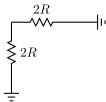
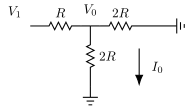
\[R_{in} = 2R \parallel 2R = R\]

16

\[R_{in} = R + R = 2R\]

\[I_{0} = \frac{V_0}{2R} = \frac{V_1}{4R}\]

17

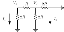
\[R_{in} = 2R \parallel 2R = R\]

\[I_{0} = \frac{V_0}{2R} = \frac{V_1}{4R}\]

\[I_{1} = \frac{V_1}{2R}\]

18

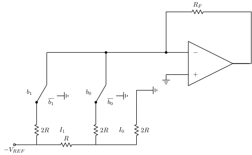
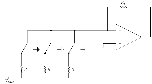
\[I_{RF} = I_1b_1 + I_0b_0 = \frac{V_{REF}}{2R}b_1 + \frac{V_{REF}}{4R}b_0\]

\[V_{O} = \left(\frac{V_{REF}}{2R}b_1 + \frac{V_{REF}}{4R}b_0\right)R_{F0}\]

19

Binary coding

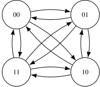
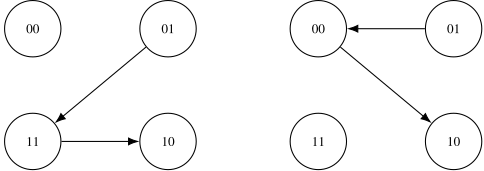
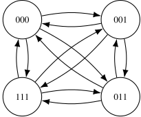
For 4 states (2-bit) there are 12 possible transitions

20

Assume MSB first (left)

\[1 \rightarrow 3 \rightarrow 2\]

Assume LSB first (right)

\[1 \rightarrow 0 \rightarrow 2\]

Both cause a non-monotonic glitch during transition.

21

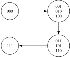
Thermometer encoding

22

The sequence of MSB to LSB does not matter.

\[0 \rightarrow 1 \rightarrow 2 \rightarrow 3\]

23
24

Current mode DACs

25
26
27

\[I_{out} = D_{in} \times I_{ref}\text{ [I]}\]

\[V_{out} = D_{in} \times V_{ref}\text{ [V]}\]

\[R_{out} = D_{in} \times R_{ref}\text{ [}\Omega\text{]}\]


\[t_{out} = D_{in} \times t_{ref}\text{ [s]}\]

\[Q_{out} = D_{in} \times Q_{ref}\text{ [C]}\]

\[V = R I\]

\(Q = C V\)

\[dt = \frac{C dV}{I}\]

\[dt = \frac{L dI}{V}\]

28

Summary

  • A DAC turns a code into charge, current or voltage by summing weighted unit elements
  • Binary weighting is compact but must switch half the array at the major carry; thermometer coding is monotonic and glitch-free but costs 2^N elements and decoding
  • Segmentation spends thermometer coding on the MSBs where it matters and binary on the LSBs where it is cheap
  • Static accuracy is INL/DNL set by element matching (Pelgrom: area buys bits); dynamic accuracy is glitch energy and SFDR
  • The references and the switch drivers are part of the DAC: their noise and timing skew show up in the output spectrum
29

Would you like to know more?

A 28-nm 75-fsrms Analog Fractional-N Sampling PLL With a Highly Linear DTC Incorporating Background DTC Gain Calibration and Reference Clock Duty Cycle Correction [@wu19]

A 10-bit Charge-Redistribution ADC Consuming 1.9 uW at 1 MS/s [@elzakker10]

A 6.3 uW 20 bit Incremental Zoom-ADC with 6 ppm INL and 1 uV Offset [@chae13]

A 12-Bit 1.25-GS/s DAC in 90 nm CMOS With >70 dB SFDR up to 500 MHz [@tseng11]

30