TFE4188 - Introduction to Lecture 2

ICs and ESD

1

Goal

Understand the real-world constraints on our IC

Understand why you must always handle ESD on an IC

2

The real world constrains our IC

3

What blocks must our IC include?

A BJT-based CMOS Temperature Sensor with Duty-cycle-modulated Output and ±0.54 °C (3-sigma) Inaccuracy from -40 °C to 125 °C [@huang21].

4
Pin Function in/out Value Unit
VDD_3V3 analog supply in 3.0 V
VDD_1V2 digital supply in 1.2 V
VSS ground in 0 V
CLK_1V2 clock in 20 MHz
RST_1V2 digital out 0 or 1.2 V
I_C bias in ? uA?
PHI1_1V2 digital out 0 or 1.2 V
PHI2_1V2 digital out 0 or 1.2 V
DCM_1V2 digital out 0 or 1.2 V

course plan

5

One more thing

6

ESD

7

Electrostatic Discharge

If you make an IC, you must consider Electrostatic Discharge (ESD) Protection circuits

Standards for testing at JEDEC

8

When do ESD events occur?

Before/during PCB

Human body model (HBM)

Charged device model (CDM)

After PCB

Human body model (HBM)

System level ESD

9

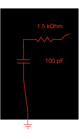
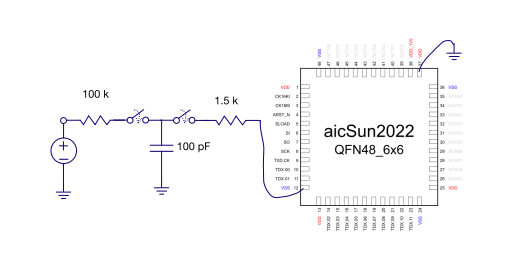
Human body model (HBM)

  • Models a person touching a device with a finger
  • Long duration (around 100 ns)
  • Acts like a current source into a pin
  • Can usually be handled in the I/O ring
  • 4 kV HBM ESD is 2.67 A peak current
10

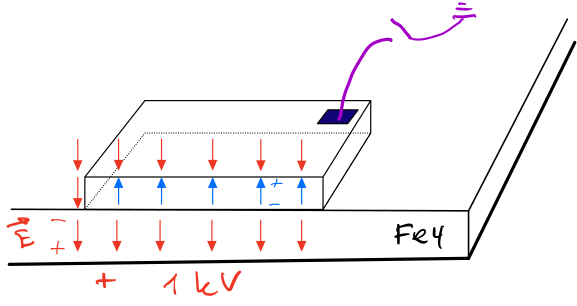
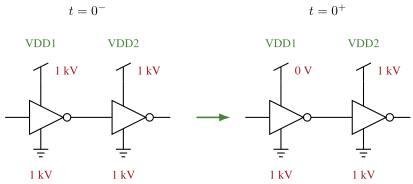
Charged device model (CDM)

Assume there is an equal number of electrons and protons on the IC. According to Gauss' law

\(\oint_{\partial \Omega} \mathbf{E} \cdot d\mathbf{S} = \frac{1}{\epsilon_0} \iiint_{V} \rho \cdot dV\)
11
12

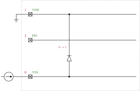
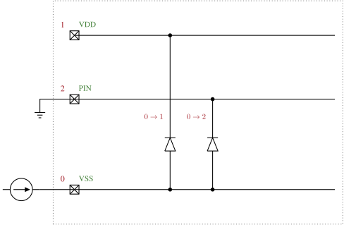
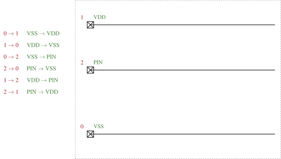
An HBM ESD zap example

Imagine a ESD zap between VSS and VDD. How can we protect the device?
13

14

15

16

17

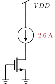
The grounded gate NMOS

18
19

If you don't do the layout right

New Ballasting Layout Schemes to Improve ESD Robustness of I/O Buffers in Fully Silicided CMOS Process [@ker09]

20

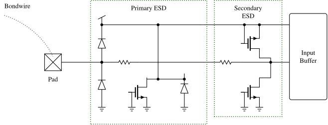
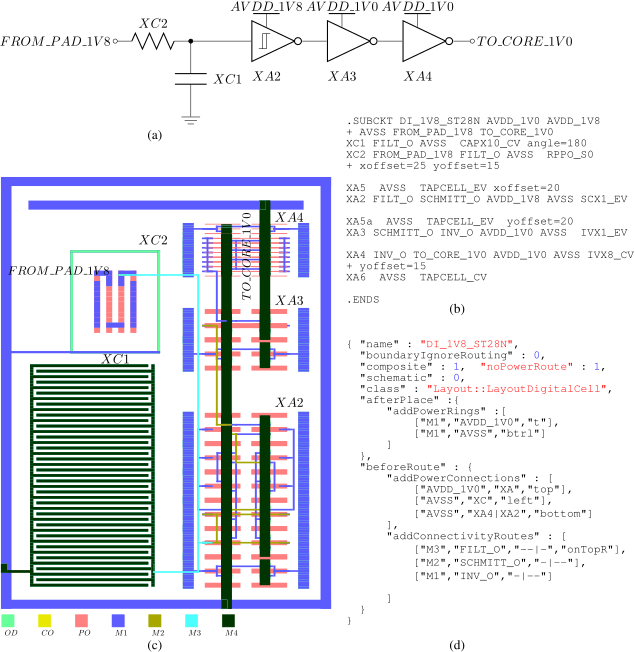
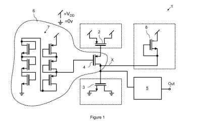
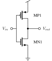
But I just want a digital input, what do I need?

21
22

Input buffer

23

Latch-up

24
25

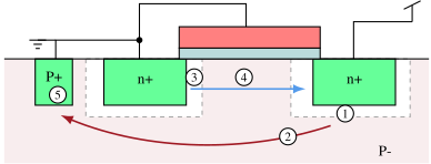
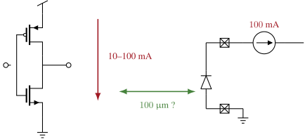
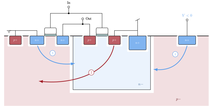
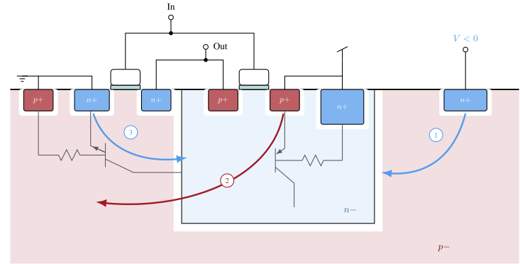
Logic cells close to large NMOS pad drivers are prone to latch-up.

The latch-up process can start with electrons injected into the p-type substrate.
26
  1. Electrons injected into substrate, diffuse around, but will be accelerated by n-well to p-substrate built in voltage. Can end up in n-well
  2. PMOS drain can be forward biased by reduced n-well potential. Hole injection into n-well. Holes diffuse around, but will be accelerated by n-well to p-substrate built in voltage. Can end up in p-substrate under NMOS
  3. NMOS source pn-junction can be forward biased. Electrons injected into p-substrate. Diffuse around, but will be accelerated by n-well to p-substrate built in voltage.
  4. Go to 2 (latch-up)
27
28
29

You must always handle ESD on an IC

  • Do everything yourself
  • Use libraries from foundry
  • Get help www.sofics.com
30

Summary

  • An ESD zap is a real event with a name: HBM is a charged person (kilovolts, amps through 1.5k), CDM is the chip discharging itself (nanoseconds, brutal)
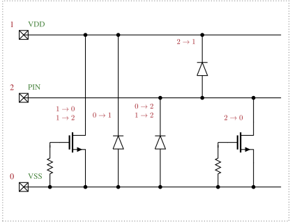
  • Protection is a promise about every ordered pair of pads: each of the six permutations on a three-pad chip needs somewhere for the current to go
  • Two diodes per pin plus one rail clamp cover all permutations - adding a pin costs two diodes, not six paths
  • The grounded gate NMOS is off by every model you were taught; the parasitic lateral bipolar is what sinks the amperes
  • Thin gate oxide cannot take the leftover voltage, so real inputs add secondary protection behind a resistor
  • Latch-up is the same parasitic bipolars firing in normal operation: keep well taps close, keep injectors away from wells
31

Would you like to know more?

Thanks!

32