Diodes

1

Why

Diodes are a magical [^1] semiconductor device that conduct current in one direction. It's one of the fundamental electronics components, and it's a good idea to understand how they work.

2

Intrinsic carrier concentration

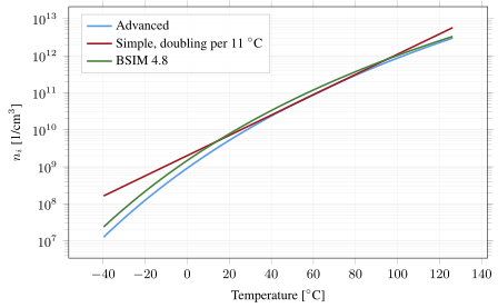
The intrinsic carrier concentration of silicon, or the density of free electrons and holes at a given temperature, is given by

\(n_i = \sqrt{N_c N_v} e^{\frac{-E_g}{2 k T}}\)

3

The density of states are

\[N_c = 2 \left[\frac{2 \pi k T m_n^*}{h^2}\right]^{3/2} \text{ } N_v = 2 \left[\frac{2 \pi k T m_p^*}{h^2}\right]^{3/2}\]

4

In BSIM 4.8 [@bsim] the intrinsic carrier concentration is

\[n_{i} = 1.45e10 \frac{TNOM}{300.15} \sqrt{\frac{T}{300.15} \exp^{21.5565981 - \frac{E_g}{2kT}}}\]
5

Density of states

\[-\frac{\hbar^2}{2m}\nabla^2\psi = E\psi\]

\[N(dk) = \frac{2}{(2 \pi)^p} dk\]

\[E(k) = \frac{\hbar^2 k^2}{2 m^*}\]

\[m^* = \frac{\hbar^2}{\frac{d^2 E}{dk^2}}\]

\[N(E)dE = \frac{\sqrt{2}}{\pi^2}\left(\frac{m^*}{\hbar^2}\right)^{3/2} E^{1/2}dE\]

6

\[f(E) = \frac{1}{e^{(E - E_F)/kT} + 1}\]

7

\[N_e dE = N(E)f(E)dE\]

8

\[n_e = 2\left( \frac{2 \pi m^\ast k T}{h^2}\right)^{3/2} e^{(E_F - E_C)/kT}\]

9

For intrinsic silicon at thermal equilibrium, we could write

\[n_0 = 2\left( \frac{2 \pi m^\ast k T}{h^2}\right)^{3/2} e^{-E_g/(2kT)}\]

10

Doping

The number of electrons and holes in a n-type material is

\[n_n = N_D \text{ , } p_n = \frac{n_i^2}{N_D}\]

and in a p-type material

\[p_p = N_A \text{ , } n_p = \frac{n_i^2}{N_A}\]

11

PN junctions

12

Built-in voltage

\[n = \int_{E_C}^{\infty} N(E) f(E) dE\]

\[n_n = e^{E_{F_n}/kT} \int_{E_C}^{\infty} N_n(E) e^{-E/kT}dE\]

\[n_p = e^{E_{F_p}/kT} \int_{E_C}^{\infty} N_p(E) e^{-E/kT}dE\]

\[\frac{n_n}{n_p} = \frac{ e^{E_{F_n}/kT}}{e^{E_{F_p}/kT}} = e^{(E_{F_n} - E_{F_p})/kT}\]

\[E_{F_n} - E_{F_p} = q\Phi\]

\[\frac{N_A N_D}{n_i^2} = e^{q\Phi_0/kT}\]

or rearranged to

\[\Phi_0 = \frac{kT}{q} ln\left( \frac{N_A N_D}{n_i^2} \right)\]

13

Current

\[\frac{p_p}{p_n} = e^{-q\Phi_0/kT}\]

\[\frac{p(-x_{p0})}{p(x_{n0})} = e^{q(V-\Phi_0)/kT}\]

\[\frac{p(x_{n0})}{p_n} = e^{qV/kT}\]

\[\Delta p_n = p(x_{n0}) - p_n = p_n\left( e^{qV/kT} -1 \right)\]

\[J(x_n) = -q D_p \frac{\partial \rho}{\partial x}\]

\[\partial \rho(x_n) = \Delta p_n e^{-x_n/L_p}\]

\[J(0) = q\frac{D_p}{L_p} p_n \left( e^{qV/kT} - 1\right)\]

14

\[I = q A n_i^2 \left( \frac{1}{N_A}\frac{D_n}{L_n} + \frac{1}{N_D}\frac{D_p}{L_p} \right)\left[ e^{qV/kT} - 1 \right]\]

15

Forward voltage temperature dependence

\[V_D = V_T \ln\left(\frac{I_D}{I_S}\right)\]

16

\[V_D = V_T \ln{I_D} - V_T \ln{I_S}\]

\[\ln{I_S} = 2 \ln{n_i} + \ln{Aq\left (\frac{D_n}{L_n N_A} + \frac{D_p}{L_p N_D}\right)}\]

\[n_i = \sqrt{B_c B_v} T^{3/2} e^\frac{-E_g}{2 kT}\]

\[B_c = 2 \left[\frac{2 \pi k m_n^*}{h^2}\right]^{3/2} \text{ } B_v = 2 \left[\frac{2 \pi k m_p^*}{h^2}\right]^{3/2}\]

\[2 \ln{n_i} = 2\ln{\sqrt{B_c B_v}} + 3 \ln T - \frac{V_G}{V_T}\]

\(V_D = \frac{kT}{q}(\ell - 3 \ln T) + V_G\)

\[\ell= \ln{I_D} - \ln{\left (Aq\frac{D_n}{L_n N_A} + \frac{D_p}{L_p N_D}\right)} - 2 \ln{\sqrt{B_c B_v}}\]

17

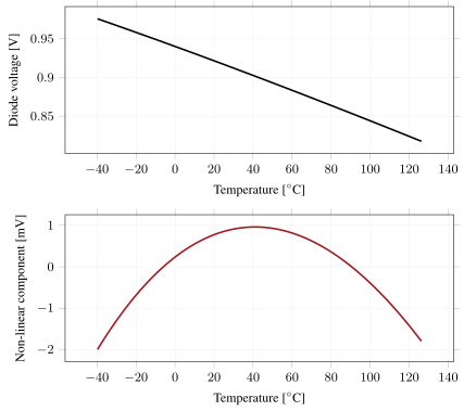
From equations above we can see that at 0 K, we expect the diode voltage to be equal to the bandgap of silicon. Diodes don't work at 0 K though.

\[\frac{dV_D}{dT} = \frac{k}{q}\bigl(\ell - 3 \ln T - 3\bigr).\]

The slope of the diode voltage can be seen to depend on the area, the current, doping, diffusion constant, diffusion length and the effective masses.
18

Current proportional to temperature

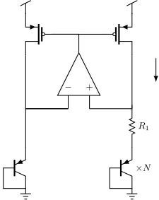
\[I_S e^\frac{qV_{D1}}{kT} = N I_S e^\frac{qV_{D2}}{kT}\]

Taking logarithm of both sides, and rearranging, we see that

\[V_{D1} - V_{D2} = \frac{kT}{q}\ln{N}\]
19

Reverse leakage

20

Diffusion leakage

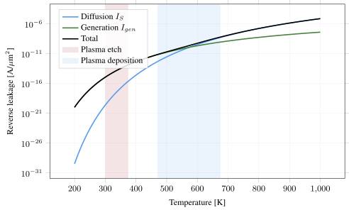
\[I_S = q A n_i^2 \left( \frac{1}{N_A}\sqrt{\frac{D_n}{\tau_n}} + \frac{1}{N_D}\sqrt{\frac{D_p}{\tau_p}} \right)\]

21

Generation in the depletion region

\[I_{gen} = \frac{q A n_i W}{\tau_g}\]

\[W = \sqrt{\frac{2 \varepsilon_{si} (\Phi_0 + V_R)}{q} \cdot \frac{N_A + N_D}{N_A N_D}}\]

22

Plasma charging currents

\[J_{plasma} \sim 1\text{-}10\, \mathrm{mA/cm^2}\]

\[I_{ant} = J_{net} \cdot A_{antenna}\]

23

Antenna ndiode, 200 K to 1000 K

24

Wires below 1 mm

\[I_{ant} = J_{net} \cdot W_{wire} \cdot L_{wire}\]

25

Thanks!

26

Summary

  • Silicon's bandgap makes it a semiconductor: few free carriers at room temperature, exponentially more when heated
  • Doping moves the Fermi level - towards the conduction band with donors, towards the valence band with acceptors
  • Join n to p and diffusion fights drift until the depletion field balances: the built-in voltage
  • Forward bias lowers the barrier exponentially: \(I = I_S(e^{V/V_T} - 1)\)
  • The diode voltage falls roughly 2 mV/K and extrapolates to the bandgap at 0 K - the seed of every bandgap reference
  • Reverse leakage grows exponentially with temperature: an antenna diode sized at etch temperature is a different diode at deposition
27

Would you like to know more?

[^1]: It doesn't stop being magic just because you know how it works. Terry Pratchett, The Wee Free Men

28